
Intel’s global push – investing billions in new production
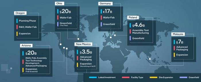
Since 2021, Intel has announced several massive projects – all in the multi-dollar scale – across the globe. From a USD 20 billion investment to build two new wafer fabs in Ohio, to a new USD 4.6 billion cutting-edge semiconductor assembly and test facility in Poland.
“Squeezing billions of tiny transistors onto ever-smaller computer chips requires one of the most complex manufacturing processes humans have devised,” that’s how Intel describes the nature of its business. And it’s hard to argue against it.
It takes roughly 6,000 construction workers three years to complete a fully equipped new fab, which also comes with a price tag of approximately USD 10 billion. Intel, being the global company that it is, operates on a massive scale – which requires a global supply chain that stretches across multiple continents.
In total, Intel is currently juggling four expansion projects and three greenfield investments, covering everything from R&D to wafer production to advanced packaging operations.
For example, Intel is investing USD 20 billion to expand its Ocotillo campus in Arizona. The company is outfitting Fab 42 with 1,300 tools, a super overhead highway that zips silicon wafers around all four of the company’s Arizona factories, and a 12-acre water plant that will treat 9.1 million gallons of wastewater a day.
In Ohio, the company is investing more than USD 20 billion to build two new fabs and to establish a new epicentre for advanced chipmaking in the Midwest. The initial phase of the project is expected to create 3,000 Intel jobs. Production is currently expected to start in 2025. Ohio will be home to Intel’s first new manufacturing site location in 40 years
In New Mexico, Intel will invest USD 3.5 billion in its operations to enable its advanced semiconductor packaging technology, Foveros. The Rio Rancho site currently develops and manufactures Intel Optane technology, embedded multi-die interconnect bridge, and Intel silicon photonics technology.
However, Intel’s investments are not just limited to the US, the company also has major plans and projects in Europe.
Intel is investing EUR 17 billion into a leading-edge semiconductor fab mega-site in Magdeburg, Germany. There are also plans to establish a new R&D and design hub in France and to expand capacities in R&D, manufacturing and foundry services in Ireland, Italy, Poland and Spain.
In Poland, Intel will invest USD 4.6 billion in a new cutting-edge semiconductor assembly and test facility in Wrocław. When completed, the facility will support approximately 2,000 Intel employees.
Earlier this year, in late September to be more precise, Intel officially opened Fab 34 in Ireland and the stated high-volume production of Intel 4 technology. This also marked the deployment of extreme ultraviolet lithography in high-volume manufacturing for the first time globally, and as the first semiconductor manufacturer in Europe.
This is the first phase of Intel’s plans to invest as much as EUR 80 billion in the EU over the next decade along the entire semiconductor value chain – from R&D to manufacturing and advanced packaging.
In Malaysia, the US chip maker is investing USD 7 billion to expand the company’s operations across Penang and Kulim.
The investment, which will expand the company’s assembly test manufacturing and also build out its die prep capability with the addition of advanced packaging capabilities, is expected to create over 4,000 new intel jobs.
According to previous reports, the new Malaysian packaging facility is expected to start production in 2024.
