

Sponsored content by AEMtec GmbH
Wafer Back-End Services at AEMtec - a closed loop for your success
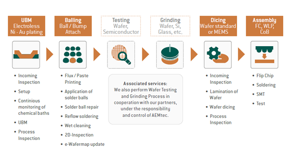
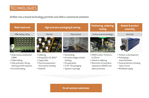
AEMtec offers their customers Back-End production stages from wafer to complex micro and optoelectronic module assembly, from one source.
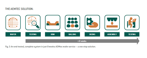
Some time ago AEMtec expanded the Wafer Back-End Services by introducing the electroless Under Bumb Metallization (UBM) and the Solder Balling processes. Significantly shorter delivery times, less workload and lower interface losses were achieved. Time-consuming intermediate steps have been eliminated. Steps that are outsourced in the typical industrial process are offered inhouse at AEMtec. Reduction of total lead time from 18 weeks to 8 weeks with the full-service AEMtec solution means faster market access for the customer`s product.
Wafer Back-end Services
AEMtec offers their customers Back-End production stages from wafer to complex micro and optoelectronic module assembly, from one source.
In year 2017 AEMtec expanded the Wafer Back-End Services by introducing the electroless Under Bump Metallization (UBM) and the Solder Balling processes. With this measure, significantly shorter delivery times, less workload, lower interface losses and costs were achieved. Many of our existing customers as well as an increasing number of new customers appreciate the shorter delivery times and generate their own competitive advantages, such as faster market access.
Typical Industry Practice
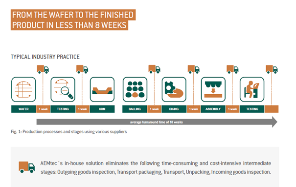 The AEMtec solution
 Why AEMtec
Commentary:
The elimination of long and frequent transport distances between the individual
production steps mean much shorter overall delivery times. Already in
the development phase of a module these shortened steps are significant. The
one-face-to-the-customer principle and its advantages already take effect in the
development phase of a module and repeat during the entire project and production
phase. In 2019 the wafer back-end capacities were extended by a new layer thickness gauge (µXRF)and by an additional wafer dicing machine. Our customers profit from the continuous
optimization of the WBS offer.
To mention only a few of the benefits by using AEMtec Wafer Back-End Services:
• Synchronized Supply Chain
• Faster time to market
• One-stop solution = process chain optimization
• Fast pre-testing possible
• No masks needed for UBM
• Only one rinsing process necessary
• Processing of several wafer lots possible
• Process reliability through fully automatic lines
• Qualified processes for balls above 50μm diameter
• Any solder alloys possible, also gold stud bumping
AEMtec Portfolio Wafer Back-end
Why AEMtec
Commentary:
The elimination of long and frequent transport distances between the individual
production steps mean much shorter overall delivery times. Already in
the development phase of a module these shortened steps are significant. The
one-face-to-the-customer principle and its advantages already take effect in the
development phase of a module and repeat during the entire project and production
phase. In 2019 the wafer back-end capacities were extended by a new layer thickness gauge (µXRF)and by an additional wafer dicing machine. Our customers profit from the continuous
optimization of the WBS offer.
To mention only a few of the benefits by using AEMtec Wafer Back-End Services:
• Synchronized Supply Chain
• Faster time to market
• One-stop solution = process chain optimization
• Fast pre-testing possible
• No masks needed for UBM
• Only one rinsing process necessary
• Processing of several wafer lots possible
• Process reliability through fully automatic lines
• Qualified processes for balls above 50μm diameter
• Any solder alloys possible, also gold stud bumping
AEMtec Portfolio Wafer Back-end
 Technologies
 Conclusion
AEMtec is one of the few full-service providers in Europe. Direct contact between our customers and engineers along with a clear structured production path shortens overall lead times and provides access to an innovatively broad technology spectrum increasing benefits for our customers, such as faster market entry, cost reduction and the receipt of high-quality products.
About us
AEMtec is a global acting specialist for the development and production of a variety of precision optoelectronic products, including components, subsystems and complete systems. With their wide range of packaging technologies AEMtec is the right partner in the sector of miniaturization.
Customer-specific requirements from the medical, industrial and automation, data and telecommunication, semiconductor as well as aerospace markets are served. AEMtec is headquartered in Berlin, Germany.
History
Established 20 years ago as spin-off from an international technology group, AEMtec focused initially on the field of unpackaged semiconductors and exclusively supplied the data and telecommunication market.
Over the last two decades, AEMtec has extensively expanded their technology portfolio, evolving into their current position as market leader in the high mix/low volume market for opto-electronic modules with annual sales of > 55 million Euro.
Contact:
AEMtec GmbH
James-Franck-Str. 10
D-12489 Berlin
Telefon: +49 30 6392 7300
E-Mail:
www.aemtec.com
Conclusion
AEMtec is one of the few full-service providers in Europe. Direct contact between our customers and engineers along with a clear structured production path shortens overall lead times and provides access to an innovatively broad technology spectrum increasing benefits for our customers, such as faster market entry, cost reduction and the receipt of high-quality products.
About us
AEMtec is a global acting specialist for the development and production of a variety of precision optoelectronic products, including components, subsystems and complete systems. With their wide range of packaging technologies AEMtec is the right partner in the sector of miniaturization.
Customer-specific requirements from the medical, industrial and automation, data and telecommunication, semiconductor as well as aerospace markets are served. AEMtec is headquartered in Berlin, Germany.
History
Established 20 years ago as spin-off from an international technology group, AEMtec focused initially on the field of unpackaged semiconductors and exclusively supplied the data and telecommunication market.
Over the last two decades, AEMtec has extensively expanded their technology portfolio, evolving into their current position as market leader in the high mix/low volume market for opto-electronic modules with annual sales of > 55 million Euro.
Contact:
AEMtec GmbH
James-Franck-Str. 10
D-12489 Berlin
Telefon: +49 30 6392 7300
E-Mail:
www.aemtec.com
The AEMtec solution
Why AEMtec
Commentary:
The elimination of long and frequent transport distances between the individual
production steps mean much shorter overall delivery times. Already in
the development phase of a module these shortened steps are significant. The
one-face-to-the-customer principle and its advantages already take effect in the
development phase of a module and repeat during the entire project and production
phase. In 2019 the wafer back-end capacities were extended by a new layer thickness gauge (µXRF)and by an additional wafer dicing machine. Our customers profit from the continuous
optimization of the WBS offer.
To mention only a few of the benefits by using AEMtec Wafer Back-End Services:
• Synchronized Supply Chain
• Faster time to market
• One-stop solution = process chain optimization
• Fast pre-testing possible
• No masks needed for UBM
• Only one rinsing process necessary
• Processing of several wafer lots possible
• Process reliability through fully automatic lines
• Qualified processes for balls above 50μm diameter
• Any solder alloys possible, also gold stud bumping
AEMtec Portfolio Wafer Back-end
Technologies
Conclusion
AEMtec is one of the few full-service providers in Europe. Direct contact between our customers and engineers along with a clear structured production path shortens overall lead times and provides access to an innovatively broad technology spectrum increasing benefits for our customers, such as faster market entry, cost reduction and the receipt of high-quality products.
About us
AEMtec is a global acting specialist for the development and production of a variety of precision optoelectronic products, including components, subsystems and complete systems. With their wide range of packaging technologies AEMtec is the right partner in the sector of miniaturization.
Customer-specific requirements from the medical, industrial and automation, data and telecommunication, semiconductor as well as aerospace markets are served. AEMtec is headquartered in Berlin, Germany.
History
Established 20 years ago as spin-off from an international technology group, AEMtec focused initially on the field of unpackaged semiconductors and exclusively supplied the data and telecommunication market.
Over the last two decades, AEMtec has extensively expanded their technology portfolio, evolving into their current position as market leader in the high mix/low volume market for opto-electronic modules with annual sales of > 55 million Euro.
Contact:
AEMtec GmbH
James-Franck-Str. 10
D-12489 Berlin
Telefon: +49 30 6392 7300
E-Mail:
www.aemtec.com