Demand from AMD and Nvidia drives FOPLP development
In 2016, TSMC developed and named its InFO FOWLP technology, and applied it to the A10 processor used in the iPhone 7. Since then, OSAT providers have been striving to develop FOWLP and FOPLP technologies to offer more cost-effective packaging solutions, TrendForce reports.
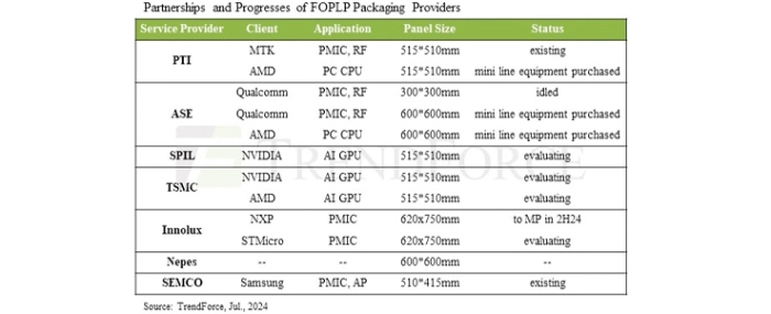
Starting in the second quarter, chip companies like AMD have actively engaged with TSMC and OSAT providers to explore the use of FOPLP technology for chip packaging and helping drive industry interest in FOPLP. TrendForce observes that there are three main models for introducing FOPLP packaging technology: Firstly, OSAT providers transitioning from traditional methods of consumer IC packaging to FOPLP. Secondly, foundries and OSAT providers packaging AI GPUs that are transitioning 2.5D packaging from wafer level to panel level. Thirdly, panel makers who are packaging consumer ICs.
Examining cases of OSAT providers transitioning from traditional packaging to FOPLP for consumer ICs, AMD has been in discussion with PTI and ASE for PC CPU products, while Qualcomm has been in talks with ASE for PMIC products. Currently, due to FOPLP’s linewidth and spacing not yet matching the level of FOWLP, FOPLP applications are temporarily limited to mature processes and cost-sensitive products like PMICs. Mainstream consumer IC products will adopt FOPLP once the technology matures.
For foundries and OSAT providers transitioning AI GPU packaging from wafer level to panel level 2.5D, AMD and Nvidia have been discussing with TSMC and SPIL for AI GPU products, focusing on enlarging the chip packaging size under the existing 2.5D model. However, due to technical challenges, foundries and OSAT providers are still evaluating this transition.
NXP and STMicroelectronics, representing the development direction of panel makers packaging consumer ICs, are currently undergoing talks with Innolux to package PMIC products.
Several points stand out regarding the impact of FOPLP technology on the packaging and testing industry: Firstly, OSAT providers can offer low-cost packaging solutions, increasing their market share in existing consumer ICs and even entering multi-chip packaging and heterogeneous integration businesses. Secondly, panel makers can enter the semiconductor packaging business. Thirdly, foundries and OSAT providers can reduce the cost structure of 2.5D packaging models, potentially expanding 2.5D packaging services from the AI GPU market to the consumer IC market. Lastly, GPU providers can increase the packaging size of AI GPUs.
TrendForce believes that the advantages and disadvantages of FOPLP — along with adoption incentives and challenges — coexist. The main advantages are lower unit costs and larger packaging sizes, but the technology and equipment systems still need development, and the commercialisation process is highly uncertain. The estimated mass production timeline for FOPLP packaging technology in consumer IC and AI GPU applications is the second half of 2024 to 2026 and 2027–28, respectively.
For more information visit TrendForce.


