



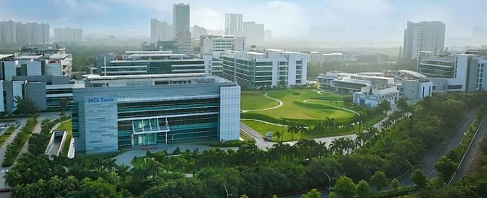
HCLTech launches semiconductor lab with $19M investment
The Advanced Semiconductor Lab in Bengaluru provides a unified platform for electrical validation, automated testing, qualification and failure analysis, streamlining the journey from design specifications to finished semiconductor parts.
HCLTech has announced the launch of its Advanced Semiconductor Lab in Bengaluru. Set up with an investment of INR 1.85 billion (about USD 19 million), the 40,000 sq ft facility features 25,000 sq ft of Class 10K and 1K cleanrooms, and delivers end-to-end post-silicon engineering, advanced testing and failure analysis, HCLTech said in a press release.
The facility is equipped with cutting-edge tools from Teradyne, Advantest, Keysight, Tektronix and Thermo Fisher Scientific Inc., supporting research and development, pre-production and production qualification, enabling faster turnaround, superior quality and reduced complexity for global customers.
The lab provides a unified platform for electrical validation, automated testing, qualification and failure analysis, streamlining the journey from design specifications to finished semiconductor parts, the company said.
“This facility reflects our deep commitment to investing in high-end engineering capabilities,” said Hari Sadarahalli, Corporate Vice President and Global Head, Engineering and R&D Services at HCLTech. “We are excited to contribute to the country’s vision of becoming a global hub for advanced technology.”
Headquartered in Noida, India, HCLTech is home to more than 223,000 people across 60 countries, delivering capabilities centered around AI, digital, engineering, cloud and software, powered by a broad portfolio of technology services and products.