

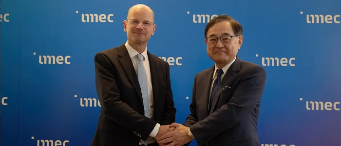
Imec sets up first R&D base in Japan, in Hokkaido
Belgian research centre Imec is setting up an R&D team in Hokkaido, Japan, focused on photonics and co-packaged optics (CPO) technologies. The team will be based at Hokkaido University in Sapporo and is to grow to around 15 researchers and engineers over five years.
The expansion is backed by Japan’s Ministry of Economy, Trade and Industry (METI) and carried out in collaboration with the Leading-edge Semiconductor Technology Center (LSTC), according to a press release from Imec. The Hokkaido team will be fully integrated into Imec’s global R&D and work closely with the teams in Leuven. According to Hokkaido University, it is Imec’s first R&D base in Japan.
The choice of focus reflects the growing importance of photonics and co-packaged optics, as the industry looks for more energy-efficient solutions for AI and high-performance computing. The team will work on photonic integrated circuits (PICs) and electronic-photonic integrated circuits (EICs), together with Hokkaido University, Tohoku University, Yokohama National University, the National Institute of Advanced Industrial Science and Technology (AIST) and the Chitose Institute of Science and Technology. Imec expects the work to support commercialisation efforts by industry partners, including Japanese chipmaker Rapidus.
“Through our R&D activities in Hokkaido, we aim to contribute to Japan’s ambitions in next-generation semiconductor and photonics technologies while further strengthening the connection between Japanese innovation and our global R&D ecosystem,” says Imec CEO Patrick Vandenameele.
The base builds on a collaboration that began when Hokkaido University and Imec signed a letter of intent in November 2024. According to the university’s president, Kiyohiro Houkin, joint projects on co-packaged optics for advanced semiconductor packaging and on medical AI use cases have started this year, and graduate students from the university have begun training at Imec.