



Aeluma buys Aixtron tool to scale photonics production without InP
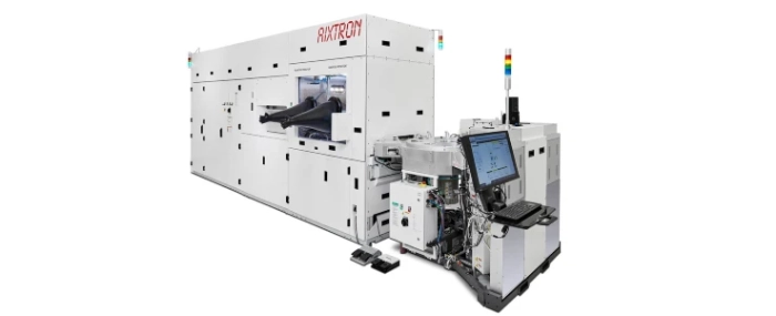
US photonics company Aeluma has bought an Aixtron G10-AsP system to expand production of photodetectors and lasers on its non-indium phosphide (non-InP) platform. The tool supports 150 mm and 200 mm wafers and has been configured for Aeluma’s own processes.
Aeluma’s technology combines certain compound semiconductor materials with microelectronics-grade gallium arsenide or silicon, according to a press release from Aixtron. That lets the company scale production to larger substrates without relying on indium phosphide substrates, and use high-volume manufacturing to achieve greater volumes and lower costs.
Aeluma was founded in 2019 as a spin-off from the University of California, Santa Barbara, and is based in Goleta, California, where it has R&D and manufacturing for wafer production, chip fabrication, prototyping and testing.
“Demand for high-speed photodetectors, quantum dot lasers and other photonic devices for AI scale-up and scale-out architectures continues to grow rapidly,” says Jonathan Klamkin, founder and CEO of Aeluma.
The order builds on several years of cooperation between the two companies. Aixtron CEO Felix Grawert says demand for photonic devices in AI is driving a shift towards larger wafer formats, and that Aeluma’s approach is a promising alternative.
Neither company discloses the value of the order or when the system will be delivered.