




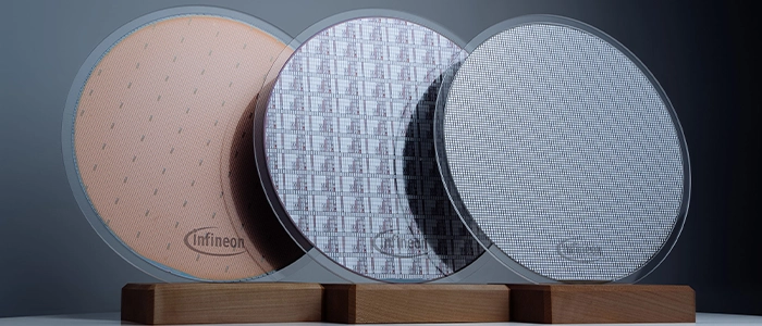
Infineon processes first 300 mm SiC wafers into working power devices
Infineon has processed 300 mm silicon carbide (SiC) wafers into functional power devices at its fab in Villach, Austria, using existing silicon manufacturing equipment. The company says it’s the first to do so in a full-scale semiconductor fab.
A 300 mm wafer gives about 2.3 times as many chips as a 200 mm wafer, according to a press release from Infineon. The company hasn’t set a timeline for volume production. It will plan the technology and ramp-up of 300 mm SiC together with customers and partners, while continuing its existing roadmap for 200 mm SiC.
In parallel, Infineon has demonstrated the feasibility of its Cold Split technology on 300 mm SiC at its site in Dresden, Germany. The method separates wafers from a SiC boule with less material loss and much shorter processing time than conventional wire sawing, so that more wafers can be obtained from the same crystal.
“With silicon, gallium nitride and now silicon carbide 300-millimeter wafers, we are in a leading position to scale semiconductor manufacturing and drive profitable growth,” says Infineon CEO Jochen Hanebeck.
Infineon now works with 300 mm wafers for all three materials. At the end of October, the company announced an investment of about EUR 1.1 billion in a high-volume plant for GaN power semiconductors on 300 mm wafers in Villach. Infineon does not say what the step means for costs.