

Applied Materials opens $5 billion EPIC Center in Silicon Valley
Applied Materials has unveiled its EPIC Center in Sunnyvale, California, where chipmakers, equipment suppliers and universities will develop new semiconductor processes alongside the company’s own engineers. TSMC, Intel, Samsung, SK hynix and Micron are among the founding partners.
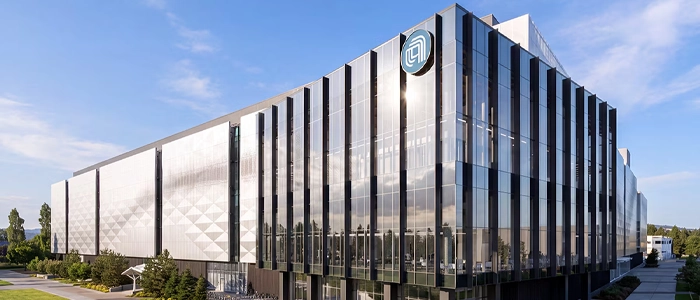
The Equipment and Process Innovation and Commercialization (EPIC) Center was unveiled on 12 October, according to a press release from Applied Materials. The company describes it as the world’s largest facility for collaborative R&D in semiconductor process technology and manufacturing equipment. The building covers around 55,700 square metres and houses roughly 1.6 hectares of cleanroom space. The investment is set at USD 5 billion – although the company states in the release that capital spending is expected to scale up to that level over time, as customer projects get under way.
The idea behind EPIC is to change how new chip technologies are developed. Traditionally, materials research, equipment and process development, and integration and pilot production take place in separate environments, with a handover between each stage. At EPIC, the people who develop the materials, build the equipment and make the chips will work in the same building.
“To win the race for AI leadership, our industry must rethink and re-engineer how we collaborate to develop and commercialize the next generation of semiconductor technologies,” said Gary Dickerson, President and CEO of Applied Materials.
Besides the five founding partners, Broadcom, Advantest, SCREEN, KIOXIA and Besi have joined as innovation partners. Arizona State University, Rensselaer Polytechnic Institute, Stanford, UC Berkeley and UCLA are taking part as research partners. Each partner brings its own engineers and technology challenges into the facility, and more companies and organisations are expected to join over time.
According to Prabu Raja, President of Applied’s Semiconductor Products Group, the main gain is that materials, processes and equipment will be developed in parallel rather than one after another.
“Because our customers’ own engineers help optimize the technology before it ever reaches their factory, what leaves EPIC arrives at the fab ready to ramp to high performance and high yield sooner,” he said.
Both sides stand to benefit. The chipmakers get early access to new materials and equipment and shorter learning cycles, while Applied gets insight into its customers’ technology challenges several generations ahead.
TSMC, which describes Applied as a partner for three decades, sees EPIC as a way to move beyond the 2-nanometre node.
“Beyond 2nm, collaborating with Applied gives us early access to the disruptive equipment technologies that define the future,” said C.C. Wei, Chairman and CEO of TSMC.