


Elephantech to open advanced packaging centre in Tokyo
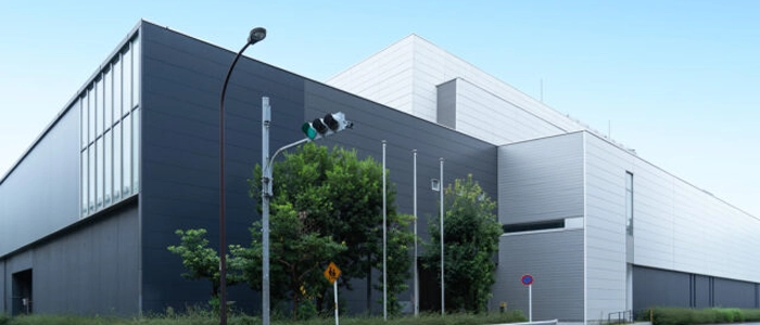
Japanese PCB and substrate technology developer Elephantech will open a new facility in Tokyo in March 2027. The Toyosu Advanced Packaging Center is intended to scale up manufacturing and advance packaging R&D for AI servers.
The centre in Koto-ku will have around 6,700 square metres of floor space, with cleanrooms, prototyping equipment for panels up to 550 × 622 mm covering everything from printing to copper electroplating, and analytical instruments, according to a press release from Elephantech. By bringing development, prototyping and evaluation together on one site, the company aims to prepare its technologies for volume production. Elephantech will also step up recruitment in materials, equipment and process development.
The company uses its own nanomaterials and precision inkjet processes to produce PCBs and package substrates with higher-density interconnects. One of its solutions, DeepVia HDI, enables metallisation of microvias with higher aspect ratios. Its DK100 equipment has already been shipped abroad for the production of AI server PCBs for an unnamed North American chipmaker. Another solution, DS-SAP, for fine-line patterning in package substrates, is being explored with North American semiconductor manufacturers to develop new substrate designs for volume production.
"Our nanomaterials technologies are emerging as key enablers for advancing AI computing performance, and we are currently working with the majority of leading AI semiconductor manufacturers on new designs," says Shinya Shimizu, CEO and founder of Elephantech.
Elephantech does not disclose the size of the investment or how many people it plans to hire.