
Intel builds the world's most advanced EUV litho machine
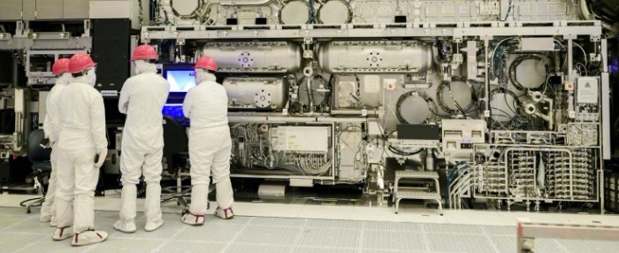
Intel's newly-formed chip foundry business says it has successfully assembled the most advanced piece of semiconductor kit ever made: a High Numerical Aperture Extreme Ultraviolet lithography scanner.
High NA EUV is the next-gen tech created by Dutch lithography specialist ASML. It is the successor to Extreme ultraviolet lithography (EUV) – a critical technique used by foundries in the manufacture of cutting-edge chips. The new High-NA machines use extreme ultraviolet light to fire a laser at a droplet of tin heated to almost 220,000 degrees Celsius. The reflected light creates a circuit pattern, which is used etch circuits onto the silicon.
Intel was the first company to buy one of the USD 373 million machines. It assembled the tool at its research and development facility in Hillsboro, Oregon, where it is now undergoing calibration steps. Intel clearly expects the tech to support its manufacture of advanced processors. It currently makes 5nm chips, but says High NA EUV lithography can help it to achieve a 1.4nm breakthrough when it moves to its new Intel 14A process in 2027.
“With the addition of High NA EUV, Intel will have the most well-rounded lithography toolbox in the industry, enabling the company to drive future process capabilities beyond Intel 18A into the second half of this decade,” said Intel Fellow and director of Lithography, Hardware and Solutions Mark Phillips.
