



FR 4 base materials: shortages, price increasing and allocations
Why PCB procurement strategies should be reviewed?
Author: Jürgen Braunsteiner, Board Member of the FED e.V.
and an Area Sales Manager at the KSG group
The PCB raw materials situation is getting more critical at the moment. Trends previously known from the components sector are now reaching the standard FR4 segment. Rising demands, shrinking stocks, longer lead times and the initial implementation of allocation programs by laminate manufacturers and fiberglass suppliers. For PCB manufacturers and their customers means material availability is becoming a decisive factor. At the same time prices are rising, driven by not only higher raw material and energy costs, but also by growing scarcity along the supply chain.
Stock Levels are fading
The currently rising demands across almost all sectors of electronics manufacturing and the pressure of rising demands for AI devices causing shrinking stock levels of FR4 base materials at raw material manufacturers and distributors. In addition, supply chains are under increasing pressure generated by various crisis. Making it impossible to refill stocks in short terms.
Allocations based on previous year volume
Allocation programs and purchasing restrictions implemented by laminate manufacturer’s presents a new challenge for PCB suppliers. Material supplies are more common based on last year purchasing volume. This is an additional challenge for PCB suppliers. The objective is understandable, to distribute materials among existing customers as fairly as possible. Problematic is, that many customers currently demands are already significantly higher than the last year’s level. Consequently, anyone requiring more today than in the past, may not receive these additional quantities, or may face delays in doing so.
Little can be done shortly to improve this fundamental market situation. But what can be done, is to „overthink“ or change technical specifications provided to the PCB supplier. Especially during periods of material shortages, it is worth reviewing whether existing specifications remains to be necessary or if they are consuming material unnecessarily.
Reconsider specifications for PCB Suppliers
Significant cost saving potential can not often be found in the electrical design, but in the manufacturing specifications. Specific panel layouts, contures or quality requirements are frequently the result of legacy practices, which never have been subsequently questioned.
However, in an era of increasing prices and material allocations, it might make sense to talk with your PCB supplier to identify opportunities for optimization.
1. Soften strict panel designs
Many customers provide their panel design to the PCB manufacturer. In many ways, it is not allowed to change anything at the panel design. Well, it make sense for the EMS-partner to use always the same size of panel, but it does not always result in an optimal material utilization.
It is always better to develop the panel design in collaboration with the PCB supplier. Every PCB manufacturer knows their own production panels, processes and machines best. They are able to propose a panel layout that might be far better suited to the available production format.
The result:
- Better panel utilization
- Less material waste
- Lower costs
- More available capacity for the same material input
Optimized layout design makes a significant difference, especially with larger production volumes.
2. Allowing X-outs in panels
If X-outs are not permitted, than this requirement should also be reviewed.
I know, a panel consisting entirely of good boards only (No X-Out) may seem attractive at first, but in practice, it often leads to a higher scrap rate and unnecessary material waste.
Here an example: A panel contains 10 PCB’s. If just a single board fails, a strict „Zero X-Out“ policy requires discarding the 9 good boards as well.
This is neither cost effective nor resource efficient.
Modern SMT machines can generally handle X-outs without difficulty. Defective PCB’s within a panel may be excluded from the assembly process by masking fiducials with marks or using other types of markers. PCB suppliers are able to offer suitable solutions for that. Permitting X-outs saves material and reduces scrap even important in a time of shortages of raw materials. This could help to produce and ship more usable PCB’S from the same amount of base materials.
3. Scoring Outlines
Conture design is another important factor. Many boards has to be fully routed even though scoring could be used for parts of the outline or even better all of the outlines.
Even PCB’s with rounded corners, bevelled edges, or specific cut-outs may be handled with hybrid solutions, such as combination of milling and scouring.
Here you may also use the rule, that the PCB supplier knows the technical capabilities of their production process best. Working together with your supplier, is always the way to find a possible solution that is perspective and efficient in terms of material usage.
Why does scoring save material?
Scoring contures can significantly reduce material consumption, because PCB’s may be placed more closely together in the production panel. When using a milling conture, a milling channel has to be allowed between the boards. This Area is wasted material.
With scoring this channel is eliminated, because the boards are placed side by side without any distance between them. This often allows placing more boards on the same production panel.
Here is an example – showing the usage on a standard PCB production panel
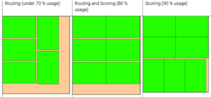
If we assume that a production panel can accommodate five units using a routed profile, six units using a mix of routing and scoring and seven units using scoring only, then a significant potential for savings becomes logical.
| Conture | Pieces per production panel | Needed production panels for supply of 1000 pcb‘s |
| Routing | 5 pieces | 200 panels |
| Routing / Scoring | 6 pieces | 167 panels |
| Scoring | 7 pieces | 142 panels |
With a fully scored conture, only 142 production panels are required in this example, instead of 200. The result is a material saving of more than 25 %. This example is presented without a specific PCB size, as every manufacturer works with their own production panel sizes. However many producers use sizes of approximately 0.5 m². When this potential for savings is applied to actual production volumes, the impact quickly makes sense.
It’s not all about the costs
Sure, such optimizations has an impact of the pcb’s price. Using less material generally leads to lower material costs. An Important factor at a time when FR4 prices are rising. But it is not all about the costs. During periods of potential supply shortages, better material utilization may help the PCB manufacturer continue to meet high volume demands. If more PCB’s can be produced from the same amount of base material, everyone in the supply chain involved would have a benefit.
There are still some more optimization opportunities.
In addition to the panel layout, X-out approval and conture design, there are some more points that should be reviewed with your supplier:
- Is the specified material thickness strictly necessary?
- Must this specific FR4 material be used, or are there other qualified alternatives?
- Is the surface technical required? Are alternatives allowed?
- Can tolerances be adjusted?
- Are there special requirements originated in the past, but not necessary anymore today?
Talk with your supplier, there will be many more points to discussed and reviewed.
Conclusion: Open Minds creates flexibility
Shortages of FR4 base materials, laminates and fiberglass are expected to continue challenging the PCB industry. Rising demands, low stock levels and allocation programs are setting prices and lead times under pressure.
This makes it all more important to have a critical look at existing requirements. Not every specification, which made sense in the past, remains to be optimal under today’s market conditions.
My tip: Get proactively in touch with your PCB Supplier. Be open to new approaches like panel layouts, X-out policies, scoring contures, material selection and surfaces. Open discussions often lead to practical solutions that may reduce costs, save material and improve supply security.
Want to hear more? Jürgen Braunsteiner will be one of the speakers at the inaugural Evertiq Expo Vienna on 4 February 2027, where he will discuss cost-effective PCB design in greater depth. Registration for the event is now open.
Based in Horn, Austria, Jürgen Braunsteiner has more than 25 years of experience in the PCB industry. As a board member of FED e.V. and Area Sales Manager at the KSG Group, he is responsible for strategic customer management and the expansion of business relationships, bringing extensive industry expertise.