
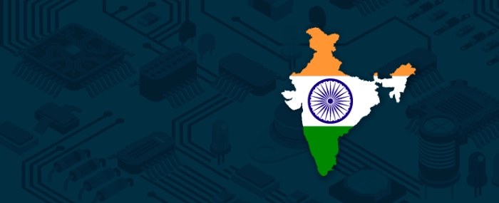
Report: $13 billion outlay for India Semiconductor Mission 2.0 cleared
India Semiconductor Mission 2.0 will be geared towards strengthening the entire semiconductor value chain, including chip design, fabrication and packaging.
The Expenditure Finance Committee (EFC) of the Indian government has approved an outlay of ₹1.25 trillion (about USD 13 billion) for the second phase of the India Semiconductor Mission (ISM 2.0), according to a report by CNBC-TV18.
This clears the way for the India Semiconductor Mission 2.0 proposal to be placed before the Union Cabinet for its consideration.
The outlay represents a hike from the first phase of the India Semiconductor Mission, for which the government had earmarked ₹760 billion (about USD 8 billion).
Sources told CNBC-TV18 that ISM 2.0 will be geared towards strengthening the entire semiconductor value chain, including chip design, fabrication and packaging.
The proposed outlay is likely to place greater emphasis on financial and non-financial incentives for compound semiconductor units, as well as manufacturers of gases, ingots and other raw materials used in chip fabrication and packaging, according to an earlier report by Business Standard.
