

IBM debuts ‘world’s first’ sub-1 nanometer chip technology
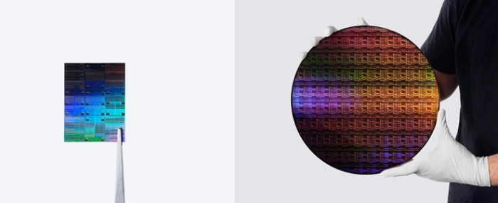
IBM’s new sub-1 nm chip packs nearly 100 billion transistors onto a chip the size of a fingernail, nearly twice the density of IBM’s 2 nm chip, unveiled in 2021.
IBM has introduced the “world’s first sub-1 nanometer (nm) chip technology,” featuring a transistor architecture at the 0.7 nm, or 7 angstrom node.
IBM’s new sub-1 nm chip packs nearly 100 billion transistors onto a chip the size of a fingernail, nearly twice the density of IBM’s 2 nm chip, unveiled in 2021. Enabled by a series of structural and material innovations, including IBM’s three-dimensional nanostack architecture, the technology demonstrates how continued gains in performance and efficiency remain possible even as chip features approach atomic dimensions, the company said in a media release.
Published technical results report the new chip is projected to offer a substantial leap in capability — up to 50 percent more performance, or 70 percent greater energy efficiency than IBM’s 2 nm node chips — supercharging compute for applications ranging from generative AI and cloud infrastructure to next-generation electronic devices.
“IBM’s latest chip breakthrough marks a landmark moment in computing, pushing technology beyond the nanometer era to the scale of atoms. With our new nanostack architecture, we’re not just making smaller transistors, we’re reinventing how chips are built to deliver dramatically more power and energy efficiency,” said Jay Gambetta, Director of IBM Research and IBM Fellow. “This industry-first innovation continues IBM’s legacy of leading in next-generation technologies and sets the foundation for the next era of computing.”
To produce this chip, IBM researchers developed an entirely new transistor architecture, called “nanostack,” the industry’s first known three-dimensional, nanosheet-based design. The nanostack design vertically stacks and staggers transistors, taking advantage of 3D sequential integration to pack more transistors onto a chip. The design also unlocks the use of different material combinations within each stacked layer, optimizing performance and power efficiency of each transistor independent of the other, IBM said.
IBM’s nanostack architecture was experimentally validated through ultra-thin dielectric bonding in CMOS integration, demonstration of dual-channel engineering capability, and functional CMOS inverter operation with expected switching performance.
