
3DGS breaks ground on chip packaging unit in India
The US company is investing about USD 21 million in the Odisha project. The facility is expected to produce 70,000 glass panels annually, along with 50 million assembled units and 13,000 advanced 3DHI modules.
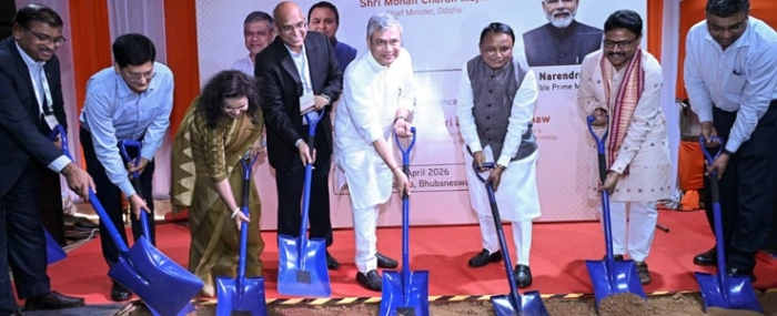
The foundation stone for India’s first advanced 3D chip packaging unit has been laid at Info Valley, Bhubaneswar, in Odisha. The project is being implemented by US company 3D Glass Solutions (3DGS) through its wholly owned Indian subsidiary Heterogeneous Integration Packaging Solutions Pvt. Ltd. (HIPSPL), according to a press release by the Indian Ministry of Electronics & Information Technology.
The company is investing nearly ₹20 billion (about USD 21 million) in the project and the facility is expected to produce 70,000 glass panels annually, along with 50 million assembled units and 13,000 advanced 3DHI modules, Odisha Chief Minister Mohan Charan Majhi said.
Majhi said the expanding semiconductor ecosystem in the state would increase employment opportunities for engineering graduates and diploma students.
Union Electronics & Information Technology Minister Ashwini Vaishnaw said two semiconductor projects have already been approved for Odisha under the India Semiconductor Mission, while three more electronics and semiconductor-related proposals are in the pipeline.
The 3DGS facility will cater to high-growth sectors such as data centres, AI, machine learning, 5G/6G communications, automotive radar, defence electronics, aerospace applications and photonics. Commercial production is expected to begin by August 2028, while full-scale volume production is targeted by August 2030, the press release said.
