

Alba PCB installs second direct imaging system at Italian facility
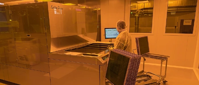
Italian PCB manufacturer Alba PCB has installed a second direct imaging (LDI) system at its production facility in Mogliano Veneto, Italy.
The installation is part of an expansion of the site’s cleanroom infrastructure, with a second Class 10,000 cleanroom now in operation. The cleanroom is designed to support advanced imaging processes for PCB manufacturing.
The newly installed system is a Ledia LDI platform supplied by Japanese Screen Research. According to Alba PCB, the system is used for direct imaging of photoresist and solder mask and is based on multi-wavelength UV-LED exposure technology.
Alba PCB states that the system enables high-resolution imaging of both iinternal and external layers of the PCB, as well as solder mask, supporting fine features and accurate pattern definition. The company also notes that the LED-based exposure technology reduces energy consumption and heat generation compared to laser-based systems.
Alba PCB said the investment is part of its efforts to maintain a high technological level at its Italian production facility.

