

Tescan expands semiconductor workflows with laser tech
By combining nanometer-level precision and high-throughput intelligent laser processing, FemtoChisel delivers pristine surfaces while significantly reducing the need for subsequent FIB polishing steps.
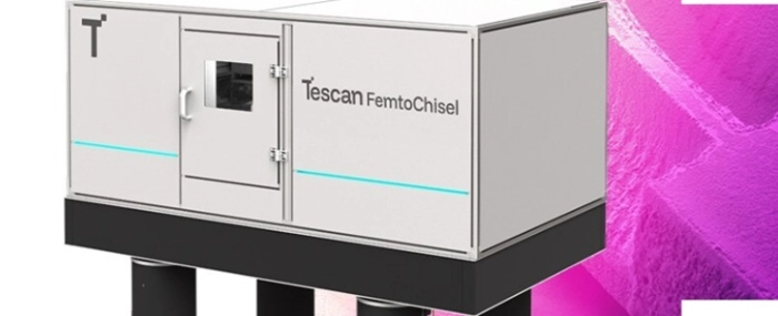
Czech company Tescan has expanded its semiconductor portfolio with FemtoChisel, a next-generation femtosecond laser platform designed to enhance semiconductor sample preparation workflows with better speed, precision, reproducibility and quality.
FemtoChisel was developed specifically for semiconductor research and failure analysis environments where both throughput and adaptability are critical, according to a press release.
By combining nanometer-level precision and high-throughput intelligent laser processing, FemtoChisel delivers pristine surfaces while significantly reducing the need for subsequent FIB polishing steps. This enables faster turnaround in research and failure analysis for current, and future, semiconductor materials.
“Semiconductor research and failure analysis teams are under constant pressure to deliver faster, more reliable results from any material layer within semiconductors stack. With FemtoChisel, we’ve addressed this challenge in our Large Volume Workflow for Semiconductors,” said Sirine Assaf, Chief Revenue Officer at Tescan.” It’s not just a new instrument — it’s a workflow enabler. By integrating ultrafast, femtosecond laser precision with intelligent adaptive laser processing, we’re helping labs accelerate sample preparation, reduce rework, and bring clarity to increasingly more complex devices.”
FemtoChisel serves both recipe-driven environments and flexible research in advanced packaging and R&D labs, providing a versatile solution for current and future semiconductor demands, the press release said.
