

Semiconductor innovation at Penn State gets $7.5M boost
Funded through the US Defense Advanced Research Projects Agency (DARPA)’s Next-Generation Microelectronics Manufacturing (NGMM) program, the work at Penn State is part of a USD 840 million multi-institutional effort.
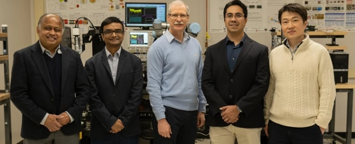
A team of researchers at Penn State has been selected to receive an award worth up to USD 5 million through the United States’ Defense Advanced Research Projects Agency (DARPA)’s Next-Generation Microelectronics Manufacturing (NGMM) program, an initiative to develop innovative semiconductor systems for the evolving demands of modern technology.
Penn State will cost share up to an additional USD 2.5 million for this project, totaling USD 7.5 million in funding, according to an online post.
Penn State’s team will tackle challenges in semiconductor design and fabrication. Specifically, the team will focus on packaging.
“The challenge in creating a microchip that is compatible with next-gen technology is packaging all the components into a small space while regulating temperature and increasing power, speed and efficiency,” said Madhavan Swaminathan, head and the William E. Leonhard Endowed Chair of the Department of Electrical Engineering. “It is like fitting a rocket engine into a shoebox but making sure it still launches without burning up the box.”
To address this, the team will emphasize the innovative use of glass packaging, which can enable improved electrical performance, better thermal isolation and is an ideal base material for the use of 3D heterogeneous integration, Swaminathan said.
The Penn State packaging research effort is part of a larger, USD 840 million investment by DARPA to the Texas Institute for Electronics (TIE) at The University of Texas (UT) at Austin. That initiative funds 32 defense electronics and commercial semiconductor companies and 18 universities, with Penn State being one of only six partner institutions from outside Texas.
Under the NGMM program, Penn State’s team will leverage its expertise to overcome key challenges in semiconductor production and design, the online post said.
The team will work to optimize the design process, material selection, performance predictions and fabrication for two major parts of semiconductors: wireless phased arrays and power converters.

