Rapidus unveils plans for new R&D facility and clean room
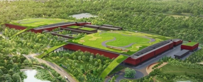
Rapidus Corporation will set up a clean room within Seiko Epson Corporation's facility in Chitose, Hokkaido, and open an R&D center for semiconductor post-processing called Rapidus Chiplet Solutions (RCS).
The Seiko Epson Chitose Plant is adjacent to the Rapidus Innovative Integration for Manufacturing (IIM) foundry, the semiconductor manufacturing facility that Rapidus is currently building in Bibi, Chitose City.
The new R&D space was unveiled at a groundbreaking ceremony held on October 3, 2024, with the clean room amassing an area of approximately 9,000 square metres. Leveraging the new R&D facility, Rapidus will develop mass production technologies for chiplet packages.
Rapidus says in a press release that it will start installing manufacturing equipment in April 2025, with R&D activities slated to begin in April 2026. The RCS will have pilot lines for the FCBGA, Si interposer, RDL, and hybrid bonding processes, and will conduct additional R&D on mass production technologies, including equipment automation.
In terms of the development of back-end processes and chiplet integration technologies, Japan's Ministry of Economy, Trade and Industry and New Energy and Industrial Technology Development Organization approved the project for the "Development of Chiplet Package Design and Manufacturing Technology for 2nm Generation Semiconductors" in April 2024, and development of core technologies such as chiplet integration and 2.5D/3D packaging is progressing.
Eralier this summer, Rapidus signed a partnership with IBM not only for front-end processes but for chiplet technology. In addition, Rapidus is collaborating with organisations across four countries, including LSTC, AIST, the University of Tokyo, Fraunhofer in Germany and A*STAR IME in Singapore to further packaging advancements.


