

© Nepes Laweh
Business |
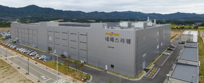
Nepes Laweh opens new 600mm PLP fab
South Korean semiconductor company, Nepes Laweh, says that it has successfully started production of the world’s first 600mm x 600mm large Panel Level Packaging (PLP) using Deca’s M-Series fan-out technologies at its newly opened Cheongan Campus.
Nepes' recently opened Cheongan Campus is built on 186,000 square metres of land, which is equivalent to 25 soccer fields. The campus is a PLP fab facility that can produce up to 96,000 of 600 mm panels with PLP per year. Nepes is expected to provide high-density packaging solutions required for advanced system semiconductors for each application, such as smartphones, automobiles, and IoT, based on the customer needs, a press release reads.
The company says that the Fan-out-Panel Level Packaging (FOPLP) line completed customer certification in the third quarter, and secured a stable yield and entered full-scale mass production.
"FOPLP is the best packaging solution for high-end semiconductors, which has resulted from of long cooperation with global partners in various industries such as materials, parts, and equipment," says Chilhee Chung, Chairman and Director of semiconductor division of Nepes in the press release.
“We’re pleased to be working with Nepes to bring the industry’s largest format 600mm square panel to volume production,” adds Tim Olson, CEO of Deca. “With initial production focused on single and multi-die packages for leading Smartphone producers, the future is heterogeneous integration of chiplets using Deca’s Gen 2 technology. A recent customer application with 10 embedded chiplets was designed into a 36mm x 36mm package. Such a large device is limited to 73% maximum utilization on 300mm round format due to edge losses. On 600mm, the utilization jumps to 92%, delivering greater than 25% cost reduction on area utilization alone.”
One of the next-generation packaging technologies, Fan-out (FO) technology can increase the number of input/output terminals by placing semiconductor I/Os outside the die. Nepes' 600mm square panel makes it possible to minimize the discarded edges and can produce five times as many chips as one 300mm round panel.