

© IBM
Components |
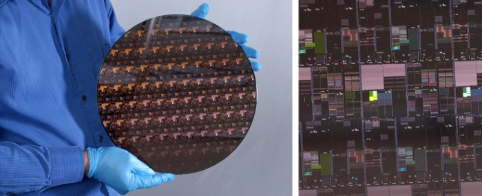
50 billion transistors on a fingernail-sized chip
IBM has unveiled a breakthrough in semiconductor design and process with the development of the world's first chip announced with 2 nanometer nanosheet technology.
Demand for increased chip performance and energy efficiency continues to rise, especially in the era of hybrid cloud, AI, and the Internet of Things. IBM is now disclosing its new 2 nm chip technology which could help the semiconductor industry addressing this growing demand. It is projected to achieve 45% higher performance, or 75% lower energy use, than today's most advanced 7 nm node chips, the company states in a press release.
"The IBM innovation reflected in this new 2 nm chip is essential to the entire semiconductor and IT industry," says Darío Gil, SVP and Director of IBM Research. "It is the product of IBM's approach of taking on hard tech challenges and a demonstration of how breakthroughs can result from sustained investments and a collaborative R&D ecosystem approach."
The breakthrough was reached at the company's research lab located at the Albany Nanotech Complex in Albany, New York, where IBM scientists work in close collaboration with public and private sector partners. The 2 nm design demonstrates the advanced scaling of semiconductors using IBM's nanosheet technology. Its architecture is an industry first. Developed less than four years after IBM announced its milestone 5 nm design, this latest breakthrough will allow the 2 nm chip to fit up to 50 billion transistors on a chip the size of a fingernail.
According to IBM, the potential benefits of these 2 nm chips could include quadrupling cell phone battery life, slashing the carbon footprint of data centers and contributing to faster object detection and reaction time in autonomous vehicles like self-driving cars.

