

© Samsung
Business |
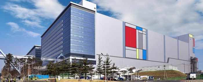
Samsung starts mass production at new EUV manufacturing line
Samsung Electronics’ new semiconductor fabrication line in Hwaseong, Korea, has begun mass production.
The facility, V1, is Samsung’s first semiconductor production line dedicated to the extreme ultraviolet (EUV) lithography technology and produces chips using process node of 7 nanometer (nm) and below. The V1 line broke ground in February 2018, and began test wafer production in the second half of 2019. Its first products will be delivered to customers in the first quarter.
“Along with technology leadership and design infrastructure, manufacturing excellence is one of the most important elements of the foundry business,” says Dr. ES Jung, President and Head of Foundry Business at Samsung Electronics, in a press release. "As we ramp up production, the V1 line will enhance our ability to respond to market demand and expand opportunities to support our customers."
The V1 line is currently producing mobile chips with 7 and 6nm process technology and will continue to adopt finer circuitry up to the 3nm process node.
By the end of 2020, the cumulative total investment in the V1 line will reach USD 6 billion in accordance with Samsung’s plan and the total capacity from 7nm and below process node is expected to triple from that of 2019. Together with the S3 line, the V1 line is expected to play a pivotal role in responding to growing global market demand for single-digit node foundry technologies.
With the V1 line in operation, Samsung now has a total of six foundry production lines in South Korea and the United States, including five 12-inch lines and one 8-inch line.
.png)