

© Kyocera
Business |
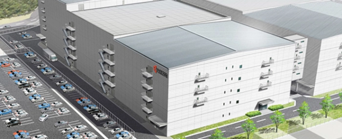
Kyocera has started building its new manufacturing plant
It was earlier this summer that the Japanese company broke ground on its new manufacturing plant for ceramic microelectronic packages in Kagoshima, Japan.
The Kagoshima Sendai facility, which Kyocera plans to open in August 2019, will bring a 25 percent increase in the company's total production capacity for ceramic packages used to house SMD electronic devices and CMOS image sensors, and will allow the company to expand production for other items depending on future needs, according to a press release.
When completed, the new six stories manufacturing facility will provide the company with a total floor space of 42’283 square metres. The company says that it has invested a total och approximately USD 53.6 million in this venture.
The electronics industry is currently experiencing new growth fueled by big data, artificial intelligence, and the Internet of Things (IoT). The development of advanced driver-assist systems (ADAS) and technology that supports minimally invasive medical treatments will drive future growth as well. The new Sendai facility will significantly increase Kyocera's production capacity for two key enablers of these applications — SMD ceramic packages and packages to house CMOS image sensors — as well as ceramic packages for automotive and medical devices.
.png)