

© Toshiba
Business |
TMC starts construction of new 3D flash memory fab
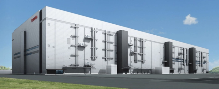
Toshiba Memory Corporation says that the company has held a groundbreaking ceremony for the first semiconductor fabrication facility (fab), called K1, in Kitakami, Iwate prefecture, in northeastern Japan.
The facility is scheduled for completion during the autumn of 2019 and will be dedicated to the production of 3D flash memory.
Demand for 3D flash memory is increasing significantly on fast growing demand for enterprise servers, datacenters and smartphones, and the company expects continued strong growth in the mid and long term. This new facility is also expected to make a major contribution to business competitiveness in corporation with Yokkaichi operations.
The new facility will be the largest Toshiba Memory fab and it will be constructed with a seismic isolation structure that allows it to absorb earthquake tremors. It will also introduce an advanced production system that uses artificial intelligence (AI) to boost productivity. Decisions on the new fab’s equipment investment, production capacity and production plan will reflect market trends, the company writes ina press release.
Toshiba Memory expects to continue its joint venture investments in the new facility based on ongoing discussions with Western Digital Corporation.
Going forward, Toshiba Memory will continue to actively cultivate initiatives aimed at strengthening competitiveness, including timely capital investments and R&D in line with market trends. The company will also contribute to the development of the regional economy of Iwate prefecture, Japan.
