

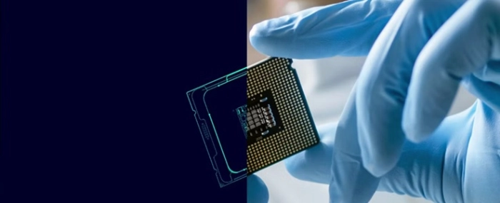
Siemens partners with Samsung Foundry to advance silicon design
Through close engineering alignment, Siemens continues to qualify and deploy its electronic design automation (EDA) software — including design, verification, simulation and silicon manufacturing enablement — with Samsung Foundry’s latest process technologies.
Siemens has announced the latest continued collaboration with Samsung Foundry, reinforcing joint efforts to enable advanced semiconductor design and manufacturing workflows for the global fabless ecosystem.
Through close engineering alignment, Siemens continues to qualify and deploy its electronic design automation (EDA) software — including design, verification, simulation and silicon manufacturing enablement — with Samsung Foundry’s latest process technologies. These efforts are focused on improving design quality, accelerating time to market and increasing confidence in first-pass silicon success at Samsung’s advanced nodes, Siemens said in a press release.
“Samsung Foundry continues to work closely with Siemens to support customers with robust, manufacturing-ready design flows across advanced process technologies,” said Hyung-Ock Kim, vice president and head of the Foundry Design Technology Team, Samsung Electronics. “Through our collaboration within the SAFE ecosystem, we are aligning proven EDA solutions with our process platforms to help customers address increasing design complexity, improve verification confidence, and accelerate innovation from design through manufacturing.”
“Our continued collaboration with Samsung Foundry reflects Siemens’ commitment to delivering production-ready EDA solutions aligned with the world’s most advanced process technologies,” said Ankur Gupta, executive vice president, IC Portfolio, Siemens EDA Siemens Digital Industries Software. “By working closely with Samsung, we are helping mutual customers to manage design complexity and bring innovative products to market with greater confidence.”

