



Huawei proposes Tau Scaling Law as successor to Moore's Law
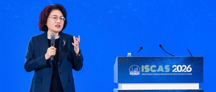
At the IEEE International Symposium on Circuits and Systems in Shanghai on May 25, Huawei presented the Tau scaling law — a new principle for guiding semiconductor development that the company proposes as a replacement for Moore's Law, which has underpinned the industry for more than five decades.
The Tau – or τ – Scaling Law was presented in a keynote by He Tingbo, President of Huawei's Semiconductor Business Department. The core proposition is a shift from geometric scaling, which has driven transistor miniaturisation under Moore's Law, to time-based scaling. Rather than measuring progress by how small transistors can be made, τ scaling measures progress by how much signal propagation delay can be reduced – compressing the time constant τ across the entire system stack, from individual transistors to interconnects, chips and computing systems.
The practical argument for the shift is that Moore's Law has run into severe physical limits and diminishing economic returns. Shrinking transistors further has become increasingly difficult and expensive, and the cost-per-transistor benefits that defined semiconductor economics for decades have largely eroded.
Huawei's application of the framework centres on a technology it calls LogicFolding, which breaks down the physical boundaries of traditional circuit layouts to significantly shorten critical-path wiring. The company also describes a multi-level co-optimisation mechanism spanning device, circuit, chip and system levels — including a new interconnect protocol called UnifiedBus for AI computing systems.
According to Huawei, the company has designed and mass-produced 381 chips based on the τ Scaling Law over the past six years. Its Kirin chips scheduled for release in autumn 2026 will be the first to use the LogicFolding architecture. By 2031, Huawei says its high-end chips designed under the τ Scaling Law are expected to achieve a transistor density equivalent to a 1.4 nanometre process.
"No single company can independently find all the answers along the path of semiconductor evolution," He Tingbo said in a press release. "With the τ Scaling Law, we look forward to working closely with scientists, engineers, and industry partners around the world."
It should be noted that the τ Scaling Law is Huawei's own framework and has not yet been independently validated or adopted by the semiconductor industry at large. The claim that it constitutes a genuine successor to Moore's Law is Huawei's own position. The transistor density projections for 2031 are likewise internal estimates.