
SCREEN’s semiconductor R&D hub opens in New York
Through this initiative, NY Creates and SCREEN Advanced Technology Center of America (ATCA) intend to connect high-tech organizations in the US and Japan to leverage their networks and drive innovation in SCREEN’s semiconductor R&D focus areas.
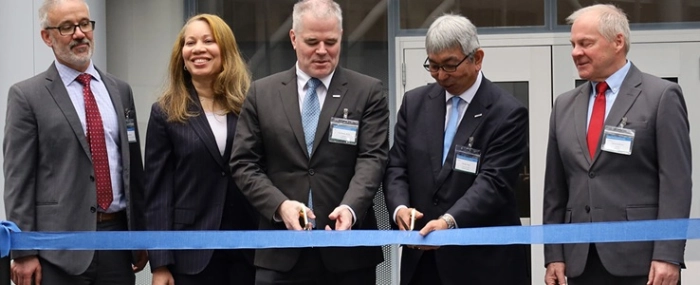
NY Creates (the New York Center for Research, Economic Advancement, Technology, Engineering, and Science) and Japanese semiconductor supply chain company SCREEN have officially opened SCREEN’s Advanced Technology Center of America, LLC (SCREEN ATCA).
SCREEN’s new research and development center is located at NY Creates’ Albany NanoTech Complex. SCREEN ATCA will leverage state-of-the-art cleanroom space within NanoFab Reflection and includes more than USD 75 million in initial investment expected during the first three years of a planned ten-year engagement, according to a media release.
“The opening of SCREEN ATCA marks yet another major milestone for New York’s globally-recognized semiconductor manufacturing industry,” New York Governor Kathy Hochul said. “This partnership allows New York to continue to expand on semiconductor innovation, creating good-paying jobs and strengthening the communities around the center.”
“With SCREEN ATCA now operational at our Albany NanoTech Complex, we are unlocking exciting opportunities for collaboration, reflecting a shared commitment to catalyze semiconductor innovation in New York for the US and the world,” NY Creates President and CEO Dave Anderson said.
“This investment will accelerate elemental technology validation and equipment development, giving us a further competitive edge and enabling us to deliver greater value to our customers,” SCREEN Holdings President and CEO and SCREEN ATCA Chairman Masato Goto said.
Through this initiative, NY Creates and SCREEN ATCA intend to connect high-tech organizations in both the US and Japan to leverage their networks and drive innovation in SCREEN’s semiconductor R&D focus areas, including semiconductor wet etch and cleaning processes with a range of wet processing, coat/develop, anneal, and image processing core technologies, the media release said.

