
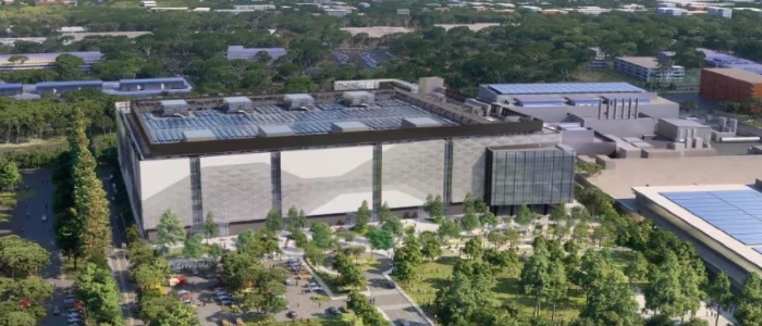
Samsung to join Applied Materials’ $5B EPIC semiconductor R&D centre
Samsung Electronics will join Applied Materials’ EPIC (Equipment and Process Innovation and Commercialisation) Centre in Silicon Valley, a semiconductor research and development facility backed by a USD 5 billion investment.
The EPIC Centre, which is scheduled to become operational in 2026, is described by Applied Materials as the world’s largest facility dedicated to collaborative R&D for semiconductor process technology and manufacturing equipment.
According to Applied Materials, Samsung will participate in joint research and development programs focused on materials engineering and process technologies for advanced logic and memory devices. The collaboration will target technologies several process nodes beyond the current generation, including new materials and atomic-scale innovations for patterning, etch and deposition, as well as future memory architectures and advanced 3D integration.
Samsung becomes the first founding member of the EPIC Centre. The two companies have an existing long-term relationship in semiconductor equipment development.
Applied Materials said the EPIC Centre is designed to dramatically reduce the time it takes to commercialise breakthrough technologies from early-stage research to full-scale manufacturing.
The facility will include cleanroom space intended for collaborative R&D between Applied Materials and its partners. Applied Materials said the EPIC model differs from traditional, sequential chip development by supporting tighter integration between equipment development and process innovation.
Applied Materials characterises the EPIC Centre as the largest investment in advanced semiconductor equipment R&D ever made in the United States.
