FAMES inaugurates pilot line in Grenoble after first validated results
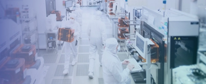
The FAMES pilot line has been officially inaugurated at CEA-Leti’s site in Grenoble, France, following the delivery of its first validated technical results. The inauguration marks the opening of a new cleanroom facility dedicated to advanced semiconductor technologies and based on 300mm semiconductor equipment.
The pilot line has been operational for two years and has delivered validated technical results in FD-SOI, RF, embedded non-volatile memories, 3D integration and power management ICs, with results presented at international conferences. The initiative is coordinated by CEA and operates as an open-access platform.
The inauguration event was attended by more than 350 participants and marked the launch of a cleanroom extension at the Grenoble site. The open-access feature of the pilot line primarily targets European start-ups, SMEs, industrial groups and research organisations seeking to prototype, qualify and reduce risk in advanced semiconductor technologies prior to industrial deployment.
CEA-Leti states that the pilot line has generated concrete advances across substrates, embedded ferroelectric non-volatile memories, advanced FD-SOI, 3D integration and high performance RF passive components.
“The breakthrough technologies developed within FAMES are intended to support future generations of sub-10nm FD-SOI chips, enabling high-performance and low-power components for Europe,” said Jean-René Lèquepeys, deputy director and CTO of CEA-Leti, in a press release. “Scaling down the FD-SOI technology to 10 and 7nm will bring significant chip performance improvements compared to current nodes, in density, power consumption, speed and radio-frequency behaviour.”
The new facility includes 2,000 square metres of cleanroom space, expanding CEA-Leti’s total cleanroom area to 14,000 square metres. It will house more than 80 300mm cleanroom tools. The building includes dedicated infrastructure for vibration control, electrical back-up systems and large-scale equipment installation.
FAMES brings together 11 partners from eight countries, and the project has a total investment of EUR 830 million, co-funded by the European Commission and participating Member States. Its stated objective is to shorten the transition from research to industrialisation while strengthening Europe’s technological autonomy in semiconductor technologies for sectors such as automotive, telecommunications, industrial systems, healthcare, space and cybersecurity.


