
STMicroelectronics to launch $60M pilot line in France
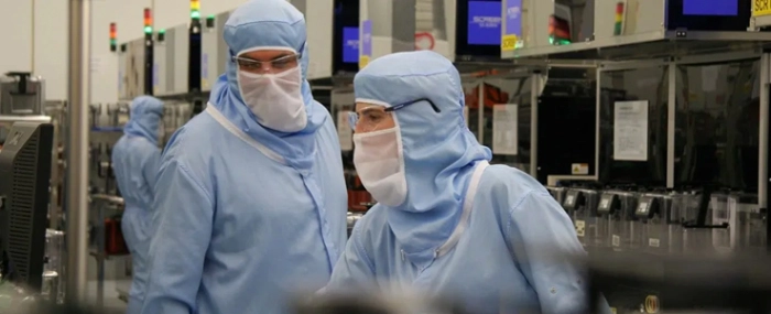
Semiconductor manufacturer STMicroelectronics plans to establish a new pilot line for Panel-Level Packaging (PLP) technology at its Tours facility in France, backed by a USD 60 million investment. The pilot line is expected to be operational in the third quarter of 2026.
PLP is an automated chip packaging and testing process designed to improve manufacturing efficiency and reduce costs. By using large rectangular carriers instead of traditional circular wafers, PLP enables higher throughput –making it an efficient solution for high-volume production.
The initiative builds on ST’s first-generation PLP line already in operation in Malaysia and is part of the company's broader strategy on heterogeneous integration, targeting applications in RF, analog, power and microcontrollers.
“The development of our PLP capabilities in Tours is aimed at advancing this innovative approach to chip packaging and test manufacturing technology, boosting efficiency and flexibility so it can be rolled out across a wide portfolio of applications,” said Fabio Gualandris, President of Quality, Manufacturing and Technology at STMicroelectronics, in a press release.
A multidisciplinary team covering experts in automation, process engineering, data science, and R&D will support the project. ST said the Tours program will leverage synergies with local research centres, including CERTEM, and contribute to reshaping its global manufacturing footprint alongside other initiatives in France and Italy.
ST previously demonstrated advanced packaging and testing capabilities at its Malta facility. The company said the new pilot line will expand its innovation capacity in Europe to support next-generation chip development across automotive, industrial, and consumer markets.
