

Blue Wave announces ‘breakthrough’ in CVD diamond research
According to the company, the DEAR MPCVD system represents the future of CVD diamond research, offering a versatile and efficient platform for exploratory and applied research in diamond-based tech.
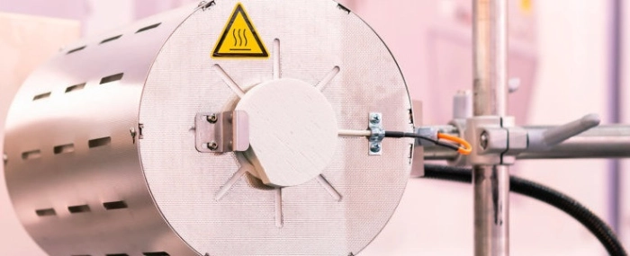
US startup Blue Wave Semiconductors has unveiled the Diamond Exploratory and Applied Research Microwave Plasma Chemical Vapor Deposition (DEAR MPCVD) system.
According to Dr. R.D. Vispute, CEO & CTO of Blue Wave Semiconductors, the DEAR MPCVD system represents the future of CVD diamond research, offering a versatile and efficient platform for exploratory and applied research in diamond-based technologies.
Blue Wave Semiconductors specializes in the development of advanced materials and technologies for next-generation applications, including quantum sensing, electronics, and composite materials.
Diamond, a wide-bandgap material, is a cornerstone for next-generation technologies, including quantum energy generation, sensing, and advanced electronics. High-quality thin films for device applications can be fabricated using Chemical Vapor Deposition (CVD) techniques, the company said.
Among these, Microwave Plasma CVD (MPCVD) reactors are the most widely used for diamond growth. To enhance the properties of diamonds for electronic and quantum applications, doping is required, which can be achieved using in-situ CVD growth with the flow of dopant gas or by the ion implantation method. However, ion implantation introduces defects in the diamond lattice, making the CVD approach more suitable for device fabrication, scalability, and high-quality diamond growth.
In this direction, Blue Wave Semiconductors has designed and developed an optimized microwave cavity that supports a larger diameter quartz tube with differential pumping vacuum seals, multiple optical viewports for temperature, plasma process, and growth monitoring, and a sample stage that creates efficient microwave plasma above the substrate (substrate size up to 12 mm x 12 mm). The system operates with various gas flow ratios, a wide range of deposition pressures, and substrate temperatures ranging from 650°C to 1100°C, enabling the deposition of homoepitaxial, large-grain microcrystalline, and nanocrystalline CVD diamond films for a variety of applications.
“Whether it’s quantum centers or doped epilayers, DEAR MPCVD delivers the precision and reliability we need. Hydrogen termination has added new dimensions to our diamond-based studies, delivering results that are beyond expectations,” said Dr. R.D. Vispute, the founder of Blue Wave Semiconductors. “The DEAR MPCVD capability to work in an R&D lab setting is a game-changer in CVD diamond research.”
