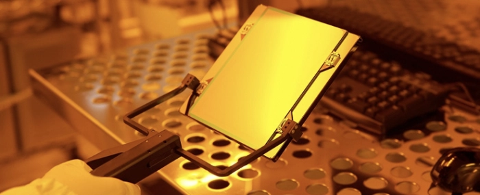
Japan’s new R&D base will introduce EUV lithography equipment
With its extremely short wavelengths of about 13.5 nanometers, EUV lithography allows for finer etching of smaller features on chips.
Japan’s National Institute of Advanced Industrial Science and Technology (AIST) is reportedly setting up a domestic research and development base for chip production equipment and semiconductor materials.
The AIST, which is affiliated with the country’s industry ministry, will be the first Japanese research institute to introduce extreme ultraviolet (EUV) lithography equipment, according to the Japan Times and Jiji Press.
With its extremely short wavelengths of about 13.5 nanometers, EUV lithography allows for finer etching of smaller features on chips. This process is not possible with conventional optical lithography.
EUV lithography equipment plays a crucial role in making chips' circuit line widths narrower.
The institute is expected to receive technical cooperation from American chipmaking giant Intel as it seeks to bolster the competitiveness of the Japanese semiconductor industry.
AIST’s new base, which will be built in three to five years, may feature a system enabling corporations to conduct experiments using EUV lithography equipment for a fee, the report said.
Measures to develop semiconductor-related personnel through exchanges with research institutes in other countries is also part of the plan.
Intel will provide expertise on chip production using EUV lithography tech.


