
Doosan Tesna to start build of $160m chip testing plant
South Korea’s Doosan Tesna is set to construct a semiconductor testing factory in Pyeongtaek, Gyeonggi Province, to meet growing demand for the inspection of new system on chip (SoC) tech.
Doosan, which specialises in plant and machinery, is expecting to break ground on the 15,870 square metre facility this year, with construction scheduled to be completed in the first half of 2027. It chose Pyeongtaek as it is also the location of one of Samsung's main memory manufacturing facilities.
The planned factory will focus on testing high-performance SoCs and CMOS image sensors. SoCs combine several components such as the central processing unit (CPU), graphics processing unit (GPU) and memory interfaces on a single substrate or microchip. A CIS is a semiconductor that takes and stores images of objects by converting light to electrical signals for each pixel.
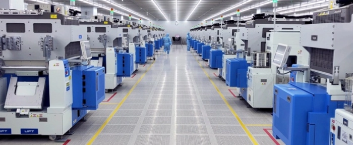
Doosan Tesna says the facility will use advanced technologies such as auto stackers, autonomous mobile robots, and solar power systems to create a smart factory environment. It will also implement vibration control technology, which is eight times stronger than standard office setups, to ensure precision in semiconductor testing.