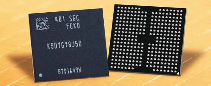
Samsung starts mass production of next-gen V-NAND
Samsung Electronics has started making 286-layer NAND flash memory chips, which expand bit density by 50% compared with 8th-generation V-NAND tech.
Competition is pretty fierce in the memory chip space, however with this announcement Samsung believes it will keep its place in or around the top of the market. It describes its new 9th-gen V-NAND as having 'the industry’s smallest cell size and thinnest mold', and cites fresh innovations such as cell interference avoidance and cell life extension.
Samsung says these features will enhance product quality and reliability while eliminating dummy channel holes. The new technology creates electron pathways by stacking mold layers and maximises fabrication productivity since it enables simultaneous drilling of the industry’s highest cell layer count in a double-stack structure.
The 9th-generation V-NAND is also equipped with the next-generation NAND flash interface, Toggle 5.1. This improves data input/output speeds by 33% to up to 3.2 gigabits-per-second (Gbps). Along with this new interface, Samsung plans to solidify its position within the high-performance SSD market by expanding support for PCIe 5.0. Power consumption has also been improved by 10%.
“We are excited to deliver the industry’s first 9th-gen V-NAND which will bring future applications leaps forward. In order to address the evolving needs for NAND flash solutions, Samsung has pushed the boundaries in cell architecture and operational scheme for our next-generation product,” said SungHoi Hur, Head of Flash Product & Technology of the Memory Business at Samsung Electronics. “Through our latest V-NAND, Samsung will continue to set the trend for the high-performance, high-density solid-state drive (SSD) market that meets the needs for the coming AI generation.”
Samsung will start mass production for the 1Tb TLC 9th-generation V-NAND this month, and the quad-level cell (QLC) model in the second half of this year.


