

ASML reaches 'first light' on High NA EUV
Dutch lithography firm ASML has confirmed that its next-gen high-numerical aperture extreme ultraviolet tool is functional.
The admission was made by the head of technology development at Intel, Ann Kelleher, during a talk at the SPIE lithography conference. Intel took delivery of its USD 400 million High-NA EUV machine late last year. In her presentation, Kelleher said the tech had seen the "first light on wafer in resist," meaning it was used in a test on a silicon wafer treated with light-sensitive chemicals and was therefore ready to receive a circuit pattern. ASML later confirmed the disclosure.
Extreme ultraviolet lithography (EUV) is a critical technique used by foundries in the manufacture of cutting-edge chips – and ASML is the only company that makes EUV machines. The new High-NA machines can print transistors 1.7 times smaller – and therefore achieve transistor densities 2.9 times higher – than today's EUV systems.
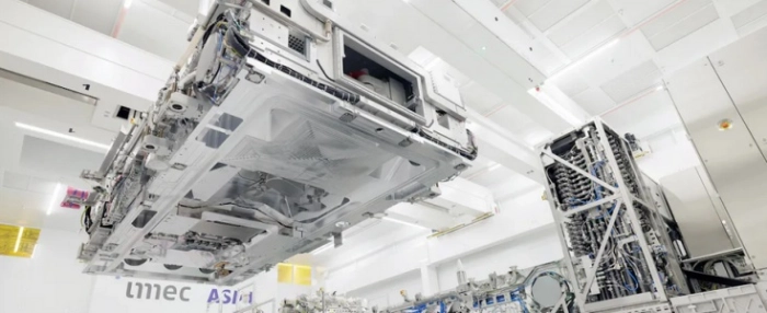
The Intel disclosure was not the only update on High NA EUV this week. Belgium's Imec demonstrated that it is ready to transfer EUV processes into the joint imec-ASML High-NA EUV Lab, built around the first prototype High-NA EUV scanner.
“The first High-NA EUV scanner has been assembled by ASML and the first wafers will be exposed soon,” says Steven Scheer, SVP of Advanced Patterning, Process and Materials at imec. “In the next few months, the joint imec-ASML High-NA EUV Lab will be operational, and access will be provided to the High-NA customers.”

