AT&S is making progress on its expansion plan
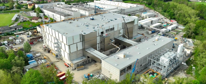
The construction cranes in Leoben Hinterberg have disappeared and the view is unobstructed again. The milestones achieved are now clearly visible. The R&D center with its series production for IC substrate technology is in according to AT&S, a lighthouse project.
“Setting up this technology outside of Asia and bringing an IC substrate production facility of this dimension to the western world for the first time is a one-of-a kind project in and for Europe,” says project leader Nikolaus Bauer-Oeppinger in a press release. “We are on schedule with the construction site and alongside the final exterior work, we started to move in the first production machines in April. Now there is nothing in the way of starting the qualification in the near future so that we can broaden our customer portfolio and supply our customers even faster and better.”
The future – EUR 500 million –R&D and IC substrate center, which will open as plant 3 alongside the two existing production facilities in Leoben Hinterberg, was put up in a record time of only 14 months. A glass and steel bridge connects the new competence center with the existing plants.
The figures associated with the project are impressive and make it the largest construction site in
At the peak of the activities in March and April, 1,100 people were working on the building site and the delivery of machines. 11,000 square metres of clean room production area were established and the gross floor area amounts to 39,000 square metres – that equals six football fields for microelectronics. Especially IC substrates – which are essential for leading-edge applications in microelectronics – will be produced in Leoben from 2024 onwards. And that is a first for Europe.
AT&S states in a press release that machines of a completely different dimension will be used for this purpose. The special machinery and equipment required for the product miniaturisation of future IC substrates allow the to advance to (PCB) substrate structures 10 times thinner than a human hair.
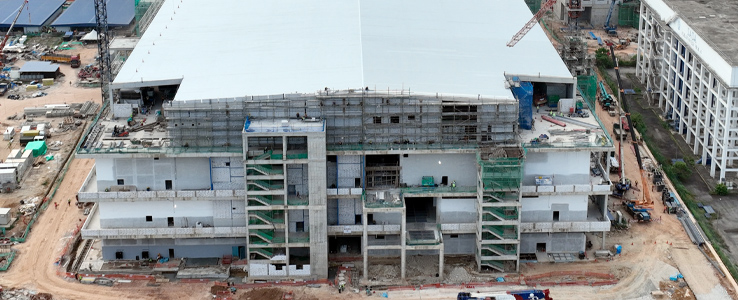
However, AT&S has another major expansion project running in parallel, the even bigger AT&S Kulim site. The company has recently celebrated the completion of the construction of the production plant and the installation of first set of tools. Production is slated to start in autumn 2024. The second production plant has been paused at the status of being wind and watertight. The company states that the ramp-up will depend on how the market develops.
The Kulim project will have a clean room area of 120,000 square metres – if you have a hard time imagining just how big that is, just think of a football field, then multiply it by 17. In just 15 months after the company broke ground, equipment is being moved in.
With the Austrian-based new production and research center of competence at the headquarters in Leoben, the new plant in Kulim and the established production sites in Chongqing, Shanghai (both China), Ansan (Korea) and Nanjangud (India) AT&S sees it self as ready for the future.


