
PCB’s made from biomaterial – a new future
What do you get from mixing one kilogram of dry beech wood shavings, about 50g of organic full-grain spelt flour, 25g of fine plaster (CaSO4) dust as well as 500g of beech wood–based inoculum?
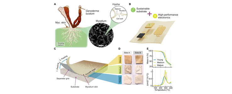
A research team from Austria developed the mix to produce biodegradable printed circuit boards that can be used, in simple electronic devices. The group from the Johannes Kepler University (JKU) Linz put the mix into a flat plastic box and stored it in a dark cupboard. Within weeks, a tissue made of fungal fibres, a so-called mycelium, grew in the box with a paper-like, soft, white to brownish skin.
The process is extremely simple and uses significantly less energy and water than circuit board production with conventional materials. In addition, there are no harmful chemicals used and the circuit boards are compostable.
Electronics production, and this is especially true for printed circuit boards, has always been challenging; it uses rare earth minerals (which come with their own set of problems) and chemicals hazardous to our health. Additionally to that, working conditions in electronics production facilities have been scrutinised for their exploitative nature. It is, mildly put, a controversial topic and we haven’t looked at environmentally-damaging chemicals that allow for the separation of some of its component materials during recycling.
Mycelial skins, like conventional printed circuit boards, can be mounted with electronic components. There is no need for new equipment and significant investments are not required. This should – in theory – make the adoption into mainstream electronics production rather easy.
How does MycelioTronics work?
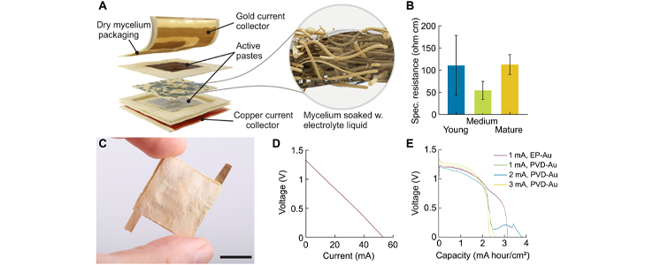
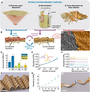
First, a wafer-thin layer of copper or gold is vapour-deposited onto the mycelium. A laser cutter is used to remove the metal wherever it is not needed. What remains are the conductor paths onto which electronic components can then be soldered.
According to the paper in Science Advances, the mycelium skin is both thin and flexible while maintaining strong structural integrity. It's been able to withstand around 2000 bending cycles; it shows only moderate resistance when folded; it insulates electrical currents; and can sustain temperatures that reach 250 degrees Celsius. Flame retardants that are ecologically and health-hazardous do not have to be added.
Real-life applications are – to date – limited in number, but the researchers successfully equipped a matchbox-sized prototype with a moisture sensor, a Bluetooth chip that can send the sensor signal to a laptop or smartphone, and a special kind of battery. However, it is currently impossible to produce multi-layer circuit boards for more complex and compact electronics. A refined formula and – with it – an even smoother mycelial skin could be a game changer: PCBs with several layers and mounted with much smaller components would be the result.
The cycle is closed with the unsoldering and recycling of the components and with the board itself being thrown into the compost. This is an advantage over so-called biopolymers, which are made from renewable raw materials such as starch or milk protein, but need an industrial composting plant and high temperatures. The metals used for the conductor paths will end up in the soil as micro-particles, but in such small quantities that they will cause no harm to the environment.
Image: (A) Possible functionalization methods of mycelium skin. (B) Formation of Cu and Cu-Au bilayer films on mycelium skin. (C) Colorized SEM image of a laser-ablated edge of a Cu-Au layer fabricated by PVD (3 nm of Cr, 400 nm of Cu, and 50 nm of Au) on a young mycelium skin (side A). Scale bar, 20 μm. (D) Conductivity of a PVD-Cu-Au layer on young, medium, and mature mycelium skin, sides A and B. n = 5. N.C., non-conducting. (E) Normalized resistance of young Cu-Au–covered mycelium during cyclic bending over 2000 times between bending radii of 5 and 25 mm. Variation of resistance in 1 cycle (gray) decreases with the number of cycles, while the maximum (blue) increases. (F) Normalized resistance of selected cycles of (E) as a function of bending radius. (G) Optical image of Cu-Au traces on a young mycelium skin after recovery of several hard folds being imposed. Scale bar, 5 mm. (H) Normalized resistance of conductor traces increases with the number of applied folds. n = 5. (I) Photograph of a young mycelium skin conductor strip with a surface mounted LED reshaped into a helix. Scale bar, 5 mm. / © Johannes Kepler University Linz
