
Global fab landscape in 2023: opportunities and challenges
The global pandemic initially caused investment to be diverted away from fab transactions, but the tenacious semiconductor industry, which is battling supply chain issues and a lack of skilled labor, has attracted new attention thanks to the potential financial support provided by U.S. and European CHIPS legislation.
In an analysis, ATREG’s President and CEO Stephen Rothrock and Yole Group’s President and CEO Jean-Christophe Eloy, discuss the emerging business models that could enable the global semiconductor industry to migrate to leading-edge and mature technology with optimal manufacturing capacity.
All segments of the semiconductor industry have seen considerable price increases during COVID, due to the limited supply chain – with the exception of the memory market. Semiconductor sales growth of 25% in 2021 is expected to fall to 11% this year, driven partly by price increases. Due to the rapid advancement of electric vehicle technology, the automotive industry in particular experienced tremendous growth. However, high demand has also caused prices in the industrial and data centre markets to rise. Inflation is another reason for slower growth, which has led to fewer orders for cellphones and other consumer goods. Blockades in the semiconductor supply chain have also occurred as a result of the war in Ukraine, along with the expansion of hyperscalers, start-up businesses, and artificial intelligence, which are all becoming more impactful areas for the industry and therefore pushing the need for more microchips around the world.
There is no doubt that recessionary winds are blowing, and chip firms must take this into account when deciding whether to increase wafer output. However, as the gentleman points out, a slower growth rate does not imply that the manufacturing needs for many companies' products will also be lower.
End-to-end design and manufacturing skills are attracting the attention of more and more businesses. Extensive R&D initiatives will benefit from cutting-edge technology, but the main problem has been the scarcity of wafer fabs at this level. The high expense of developing fabs and bringing them online is a big factor in why there aren't many of them in the globe.
Government incentives will undoubtedly be helpful, but China has already committed about USD 73 billion in semiconductor subsidies (not including grants, equity investments, and low-interest loans totaling more than USD 50 billion), while the United States, Europe, and Japan have not been able to match that amount.
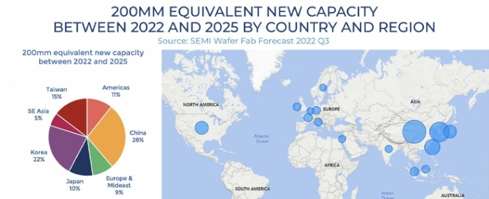
No significant investment consolidation has occurred over the past three quarters, and as a result, everyone is investing to catch up. Due to the need for more cutting-edge devices, production must be further increased. With only a little more than 150 300mm fabs worldwide – with 42 of them located Taiwan, 33 in China, 19 in the United States, and only 12 in Europe and the Middle East – the supply is constrained. Although leading edge is crucial and draws a lot of investment, a substantial percentage of activity still occurs at 200mm, with demand being greatest for various nodes from 90nm to 180nm processes. There are around 230 200mm fabs globally, 51 of which are in the United States and 49 n Europe and the Middle East.
The construction of new fabs – being built at advanced geometries – must be balanced with the long-term requirement for manufacturing at nodes with less advanced nodes. According to the gentleman, the current environment is pushing chip companies to work smarter and join forces in order to make the most of their limited resources and reduce manufacturing costs; one such cooperation is that between ST Microelectronics and GlobalFoundries.
Visit © Yole Group for the full analysis.
