
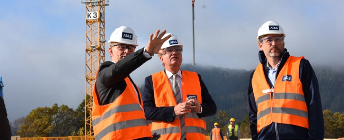
Machines will move in at AT&S Leoben in early 2023
AT&S is currently building a EUR 500 million, microelectronics R&D centre at the company headquarters in Leoben, Austria. Construction is on schedule and the first machines will arrive in early 2023.
The company is creating new capacities at Leoben for the production of IC substrates, which are an integral part of modern high-performance microchips and for advanced packaging solutions.
As a result, the region Styria will become a central location for the growing European semiconductor industry, according to a company press release.In the future, IC substrates from Leoben will not only be supplied to chip manufacturers. The company is also looking for close cooperations with universities and research institutions such as Silicon Austria Labs (SAL).
As part of the IPCEI initiative launched by the European Union to promote innovative investments ("Important Projects of Common European Interest"), the Austrian government has already pledged to make funds available to technology companies as part of "IPCEI Microelectronics 2".
"It is crucial that the Austrian government not only supports research but also the domestic technology companies accordingly."“When talking about a 'green transformation', you have to understand that technology and especially microelectronics will play a major role here. Intelligent controls and efficient systems will allow societies to act more sustainably in the future without sacrificing growth," AT&S CEO Andreas Gerstenmayer underlined the importance of this promise.
In addition to the supra-regional importance of the new microelectronics centre in Leoben-Hinterberg, the additional capacities at AT&S also increase the attractiveness of the region for potential job seekers. The expansion of the Leoben site will create 800 new positions.
