

© Leica
PCB |
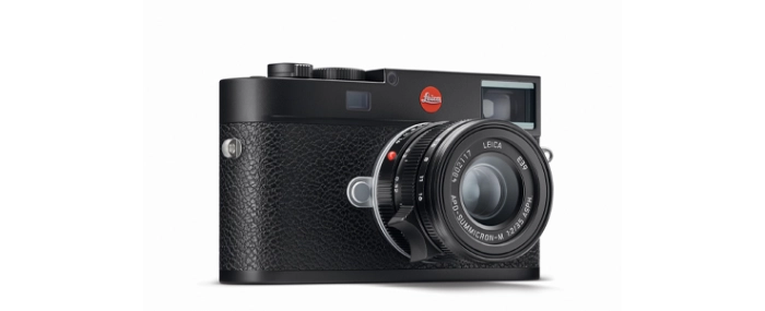
Twelve different AT&S PCB's in Leica's M11 model
German camera manufacturer Leica has released its latest camera, the Leica M11, for which Austrian PCB manufacturer AT&S acted as a development partner of PCB and interconnection technologies.
With the new M generation Leica offer the user a full-frame BSI CMOS sensor with triple resolution technology; raw files in DNG format or JPEGs can be created with a resolution of either 60, 36, or 18 megapixels.
This is where AT&S work comes into play. A total of twelve different AT&S circuit boards are included in the new M11, including the solutions for integrating the image sensor and image processing.
“The trust that a premium manufacturer like Leica places in AT&S products and solutions once again confirms our company’s solution expertise and technological capabilities,” says AT&S CEO Andreas Gerstenmayer in a short update.
The PCB's for the Leica M11 are manufactured both at the Hinterberg site and at the AT&S plant in Korea.

