
Nano Dimension set up lab to advance multi-layer printed electronics
In a collabotation with TTM Technologies, Nano Dimension plans to open its first AME NanoLab at TTM’s Advanced Manufacturing Center in Stafford Springs, Connecticut.
The aim of the NanoLab is to enable customers and researchers to actively experience the complete Additively Manufactured Electronics workflow in two steps, from design to final prototype. Experts will be on hand to work one-on-one with defense, aviation, aerospace, medical, advanced industrial, and research users to support them in accelerating the development cycles for novel electronic products.
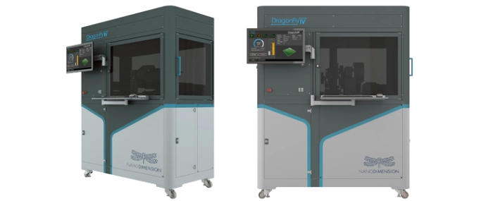
By launching the first site, named AME NanoLab @ TTM, Nano Dimension and TTM intend to drive growth and new capabilities in the AME market. The alliance will draw upon TTM’s expertise in the PCB industry, TTM already owns and operates three Nano Dimension DragonFly systems at its manufacturing center.
“3D printed electronics are rapidly evolving, delivering a step-change in electronics manufacturing,” stated Sean Patterson, President of Americas, Nano Dimension in the press release. “With this industry-leading partnership, we’re launching our first AME NanoLab Network site. Our goal is to align roadmaps, research, and development to support TTM and their original equipment manufacturers (OEMs), which will provide a better understanding of their use cases and materials requirements.”
“We are excited to have a NanoLab in our Advanced Manufacturing Center,” adds Phil Titterton, Chief Operating Officer, TTM. “Our work with Nano Dimension’s equipment will complement our other efforts in additive electronics manufacturing as well as our larger Industry 4.0 efforts at TTM.”