© AT&S Austria Technologie & Systemtechnik AG
PCB |
New office building for AT&S in Austria
The production of printed circuit boards and the expansion of the business and technology portfolio to include IC substrates, which began a few years ago, make it necessary to create additional production areas, according to the company.
"Our company has, due to our strategic direction, grown enormously in recent years," says AT&S CEO Andreas Gerstenmayer. "On the one hand, we were able to achieve a position at the top of the world in the high-tech circuit board segment and, on the other hand, we managed to expand our business and technology portfolio to include IC substrates."
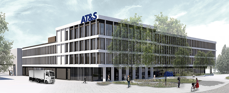
In order to meet the increasing space requirements, AT&S decided to build a contemporary and modern new office building in Leoben (Austria). In the new office building, a total of 8,322 square meters of office space will be created for around 300 newly created and existing job positions. This means that the areas that are currently used as offices can be re-allocated - again - for circuit board production.
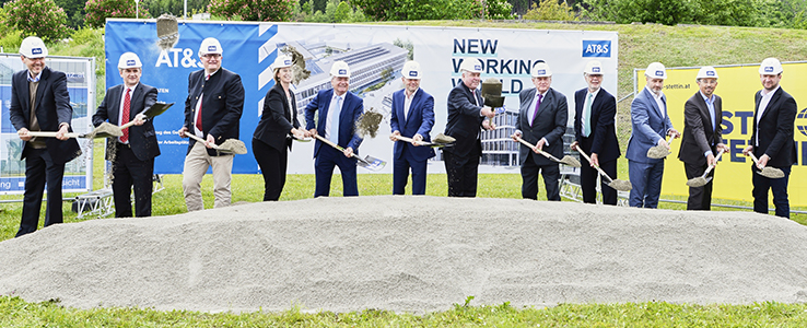
The start of construction for the new AT&S office building is scheduled for June 2021 and completion is planned for summer 2022.
As communicated in the previous year, the Leoben-Hinterberg location is investing in a major technology upgrade of up to EUR 120 million, around EUR 20 million of which will flow into R&D and around EUR 100 million will be used to purchase machines and implement new processes. "Here in Leoben, we produce the carrier material that forms the basis for IC substrates that we manufacture in our Chinese plant in Chongqing and are used in high-performance computers such as servers," says Simon Sebanz, Head of the AT&S Leoben-Hinterberg site.


