
© Christian Koenen GmbH
PCB |
High Precision Stencil Printing needs 3D Printing Tools
According to several studies, roughly half of all soldering defects occurring in SMD assembly production are still closely related with the printing of the soldering paste.
This is a product release announcement by Christian Koenen GmbH. The issuer is solely responsible for its content.
Essential therefore for a high yield is the most suitable choice of high precision stencil printer, adapted printing parameters as well as the optimal precision stencil. Highly precise milled stepped stencils offer a very efficient and economical option for the optimal application of soldering paste. But a stepped stencil is not just a stepped stencil.
The volume of the soldering paste deposit is determined significantly by the material thickness of the printing stencil used.
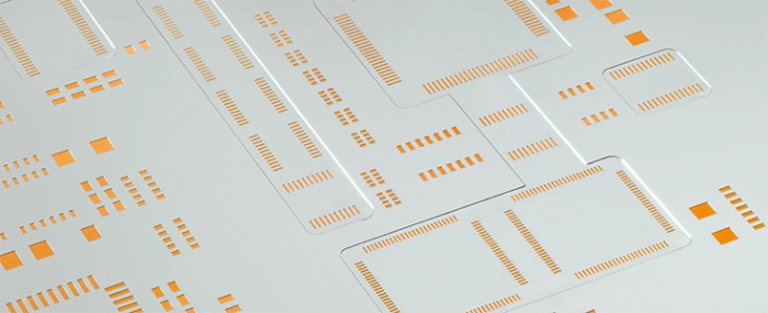
 Image 1:Stepped stencils are used, when the applied quantity of paste can no longer be adequately regulated via the adjustments of the apertures.(© Christian Koenen GmbH)
In other words, if on a circuit board components with a height variance with regard to the component size resp. the soldering paste requirement (unfavorable component mix) are planned, the respective optimal deposit volume can no longer be produced with a conventional stencil (insufficient amount of paste).
"Components such as SMD circuit board connection terminals represent particular challenges, because they very frequently feature deviations of the contact surfaces of the component of up to 100 μm to one another resp. to the contact surface." stated Sebastian Bechmann, Application Manager of the Christian Koenen GmbH. They require a stencil thickness of about 150 to 200 μm (defective coplanarity). In contrast the deposits for SMD components of the sizes 0402 can best be printed with 120 to 150 μm thick stencils. One also frequently finds insufficient amounts of paste in the combination μBGA and connector or SMT-components and THR-components.
Patented, milled and laser-cut high precision stepped stencils
Also when Fine-Pitch components are placed close together with standard components (mixed configuration), the conventional stencils come up against their limits and can, for example, cause a bridge-short-circuit formation. Especially with mixed configurations with small grid sizes and a high number of components, a high precision milled and laser-cut stepped stencil from Christian Koenen GmbH, optimally adapted to the layout is often the most efficient and economical option in order to avoid soldering defects right from the start.
Image 1:Stepped stencils are used, when the applied quantity of paste can no longer be adequately regulated via the adjustments of the apertures.(© Christian Koenen GmbH)
In other words, if on a circuit board components with a height variance with regard to the component size resp. the soldering paste requirement (unfavorable component mix) are planned, the respective optimal deposit volume can no longer be produced with a conventional stencil (insufficient amount of paste).
"Components such as SMD circuit board connection terminals represent particular challenges, because they very frequently feature deviations of the contact surfaces of the component of up to 100 μm to one another resp. to the contact surface." stated Sebastian Bechmann, Application Manager of the Christian Koenen GmbH. They require a stencil thickness of about 150 to 200 μm (defective coplanarity). In contrast the deposits for SMD components of the sizes 0402 can best be printed with 120 to 150 μm thick stencils. One also frequently finds insufficient amounts of paste in the combination μBGA and connector or SMT-components and THR-components.
Patented, milled and laser-cut high precision stepped stencils
Also when Fine-Pitch components are placed close together with standard components (mixed configuration), the conventional stencils come up against their limits and can, for example, cause a bridge-short-circuit formation. Especially with mixed configurations with small grid sizes and a high number of components, a high precision milled and laser-cut stepped stencil from Christian Koenen GmbH, optimally adapted to the layout is often the most efficient and economical option in order to avoid soldering defects right from the start.
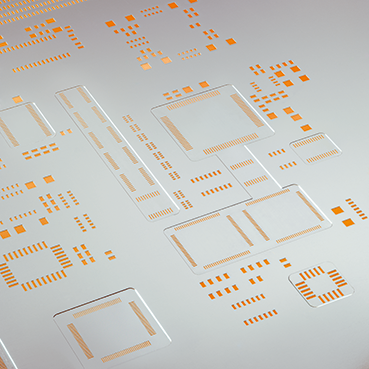 Image 2: Stepped stencils realize the compensation of differences in height in the circuit board surface, so that an artificial jump and the associated print smearing are avoided. (© Christian Koenen GmbH)
Besides the mixed configuration there are other indicators that favor the use of a stepped stencil. Such as when soldering paste is to be applied to different levels. This is required, for example, when individual components are to be sunk in the circuit board or circuit board areas of different thickness, such as rigid and flexible circuit board areas of an assembly are to be printed in one operation (sunken components).
During the course of the technological further development in the area of circuit boards and components, new challenges emerge for the high precision printing. When the circuit board to be printed features particularly sensitive areas such as bonding surfaces, chip mounting (Attach) or point protrusions due to substrate unevenness, excessively high solder resist or protruding via plug, a conventional printing stencil can be damaged in sensitive areas. "More and more frequently unwanted uncontrolled jumps within the stencil image develop after multiple use" referred Sebastian Bechmann, Application Manager of Christian Koenen GmbH. More frequent cleaning cycles, printing defects or even damage to the assembly can be the result. Stepped stencils provide a solution here too: These can be provided with cavities at critical areas, which protect the sensitive areas or compensate unevenness in the substrate (unevenness on the circuit board).
In addition the CK stepped stencils enable a combination print: Some SMT shapes must be fixed on the circuit board, so that they cannot lift up or move during the soldering process. With the help of the stepped stencil, here the adhesive can be applied directly after the printing of the soldering paste (print on print).
"Due to the uninterrupted trend towards higher and higher packing density, increased component mix as well as towards the use of smaller and smaller components, an increasing significance of the stepped stencil is to be reckoned with in the assembly production" stated Michael Brianda, CEO of Christian Koenen GmbH. The rapidly rising number of assemblies also features several of the challenges described, for which the high precision stepped stencils of the company will be used more and more frequently.
Image 2: Stepped stencils realize the compensation of differences in height in the circuit board surface, so that an artificial jump and the associated print smearing are avoided. (© Christian Koenen GmbH)
Besides the mixed configuration there are other indicators that favor the use of a stepped stencil. Such as when soldering paste is to be applied to different levels. This is required, for example, when individual components are to be sunk in the circuit board or circuit board areas of different thickness, such as rigid and flexible circuit board areas of an assembly are to be printed in one operation (sunken components).
During the course of the technological further development in the area of circuit boards and components, new challenges emerge for the high precision printing. When the circuit board to be printed features particularly sensitive areas such as bonding surfaces, chip mounting (Attach) or point protrusions due to substrate unevenness, excessively high solder resist or protruding via plug, a conventional printing stencil can be damaged in sensitive areas. "More and more frequently unwanted uncontrolled jumps within the stencil image develop after multiple use" referred Sebastian Bechmann, Application Manager of Christian Koenen GmbH. More frequent cleaning cycles, printing defects or even damage to the assembly can be the result. Stepped stencils provide a solution here too: These can be provided with cavities at critical areas, which protect the sensitive areas or compensate unevenness in the substrate (unevenness on the circuit board).
In addition the CK stepped stencils enable a combination print: Some SMT shapes must be fixed on the circuit board, so that they cannot lift up or move during the soldering process. With the help of the stepped stencil, here the adhesive can be applied directly after the printing of the soldering paste (print on print).
"Due to the uninterrupted trend towards higher and higher packing density, increased component mix as well as towards the use of smaller and smaller components, an increasing significance of the stepped stencil is to be reckoned with in the assembly production" stated Michael Brianda, CEO of Christian Koenen GmbH. The rapidly rising number of assemblies also features several of the challenges described, for which the high precision stepped stencils of the company will be used more and more frequently.
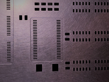 Image 3: Stepped stencil with Plasma Coating: The printing process is improved considerably and thus increases the output of the production line. (© Christian Koenen GmbH)
High precision stepped stencil with Plasma 3 coating
More and more users profit from another innovation from the house of Koenen: The milled, laser-cut stepped stencil with Plasma 3 coating. Thereby, with a plasma-supported chemical vapor deposition a coating is applied reproducibly to the substrate side and in the apertures, which improves the transfer behavior of the soldering paste (defective paste-release behavior). In the meantime the CK-Team has already brought the third generation of the Plasma Coating (Plasma 3.0) onto the market, which is remarkably distinguished in particular in the smallest apertures through very low adhesion forces. The smearing of the paste on the circuit board side is reduced and the number of cleaning cycles can be reduced, resulting in savings for production costs as well as throughput time. In addition the coating, which is only a few nanometers in thickness, is chemically and mechanically resistant. This results in fewer stoppages for stencil cleaning.
Electronics production with fully automated printing process
The real challenges in the high precision printing process listed here not only occur individually, rather increasingly also in various combinations:
Image 3: Stepped stencil with Plasma Coating: The printing process is improved considerably and thus increases the output of the production line. (© Christian Koenen GmbH)
High precision stepped stencil with Plasma 3 coating
More and more users profit from another innovation from the house of Koenen: The milled, laser-cut stepped stencil with Plasma 3 coating. Thereby, with a plasma-supported chemical vapor deposition a coating is applied reproducibly to the substrate side and in the apertures, which improves the transfer behavior of the soldering paste (defective paste-release behavior). In the meantime the CK-Team has already brought the third generation of the Plasma Coating (Plasma 3.0) onto the market, which is remarkably distinguished in particular in the smallest apertures through very low adhesion forces. The smearing of the paste on the circuit board side is reduced and the number of cleaning cycles can be reduced, resulting in savings for production costs as well as throughput time. In addition the coating, which is only a few nanometers in thickness, is chemically and mechanically resistant. This results in fewer stoppages for stencil cleaning.
Electronics production with fully automated printing process
The real challenges in the high precision printing process listed here not only occur individually, rather increasingly also in various combinations:
Image 1:Stepped stencils are used, when the applied quantity of paste can no longer be adequately regulated via the adjustments of the apertures.(© Christian Koenen GmbH)
In other words, if on a circuit board components with a height variance with regard to the component size resp. the soldering paste requirement (unfavorable component mix) are planned, the respective optimal deposit volume can no longer be produced with a conventional stencil (insufficient amount of paste).
"Components such as SMD circuit board connection terminals represent particular challenges, because they very frequently feature deviations of the contact surfaces of the component of up to 100 μm to one another resp. to the contact surface." stated Sebastian Bechmann, Application Manager of the Christian Koenen GmbH. They require a stencil thickness of about 150 to 200 μm (defective coplanarity). In contrast the deposits for SMD components of the sizes 0402 can best be printed with 120 to 150 μm thick stencils. One also frequently finds insufficient amounts of paste in the combination μBGA and connector or SMT-components and THR-components.
Patented, milled and laser-cut high precision stepped stencils
Also when Fine-Pitch components are placed close together with standard components (mixed configuration), the conventional stencils come up against their limits and can, for example, cause a bridge-short-circuit formation. Especially with mixed configurations with small grid sizes and a high number of components, a high precision milled and laser-cut stepped stencil from Christian Koenen GmbH, optimally adapted to the layout is often the most efficient and economical option in order to avoid soldering defects right from the start.
Image 2: Stepped stencils realize the compensation of differences in height in the circuit board surface, so that an artificial jump and the associated print smearing are avoided. (© Christian Koenen GmbH)
Besides the mixed configuration there are other indicators that favor the use of a stepped stencil. Such as when soldering paste is to be applied to different levels. This is required, for example, when individual components are to be sunk in the circuit board or circuit board areas of different thickness, such as rigid and flexible circuit board areas of an assembly are to be printed in one operation (sunken components).
During the course of the technological further development in the area of circuit boards and components, new challenges emerge for the high precision printing. When the circuit board to be printed features particularly sensitive areas such as bonding surfaces, chip mounting (Attach) or point protrusions due to substrate unevenness, excessively high solder resist or protruding via plug, a conventional printing stencil can be damaged in sensitive areas. "More and more frequently unwanted uncontrolled jumps within the stencil image develop after multiple use" referred Sebastian Bechmann, Application Manager of Christian Koenen GmbH. More frequent cleaning cycles, printing defects or even damage to the assembly can be the result. Stepped stencils provide a solution here too: These can be provided with cavities at critical areas, which protect the sensitive areas or compensate unevenness in the substrate (unevenness on the circuit board).
In addition the CK stepped stencils enable a combination print: Some SMT shapes must be fixed on the circuit board, so that they cannot lift up or move during the soldering process. With the help of the stepped stencil, here the adhesive can be applied directly after the printing of the soldering paste (print on print).
"Due to the uninterrupted trend towards higher and higher packing density, increased component mix as well as towards the use of smaller and smaller components, an increasing significance of the stepped stencil is to be reckoned with in the assembly production" stated Michael Brianda, CEO of Christian Koenen GmbH. The rapidly rising number of assemblies also features several of the challenges described, for which the high precision stepped stencils of the company will be used more and more frequently.
Image 3: Stepped stencil with Plasma Coating: The printing process is improved considerably and thus increases the output of the production line. (© Christian Koenen GmbH)
High precision stepped stencil with Plasma 3 coating
More and more users profit from another innovation from the house of Koenen: The milled, laser-cut stepped stencil with Plasma 3 coating. Thereby, with a plasma-supported chemical vapor deposition a coating is applied reproducibly to the substrate side and in the apertures, which improves the transfer behavior of the soldering paste (defective paste-release behavior). In the meantime the CK-Team has already brought the third generation of the Plasma Coating (Plasma 3.0) onto the market, which is remarkably distinguished in particular in the smallest apertures through very low adhesion forces. The smearing of the paste on the circuit board side is reduced and the number of cleaning cycles can be reduced, resulting in savings for production costs as well as throughput time. In addition the coating, which is only a few nanometers in thickness, is chemically and mechanically resistant. This results in fewer stoppages for stencil cleaning.
Electronics production with fully automated printing process
The real challenges in the high precision printing process listed here not only occur individually, rather increasingly also in various combinations:
- insufficient amount of paste
- defective coplanarity of the component contacts
- bridge-short-circuit formation
- sunken components
- unevenness on the circuit board
- print on print
- poor paste-release behavior from the stencil opening
- high number of down times for stencil cleaning