

© Jenoptik (illustration purpose only)
Electronics Production |
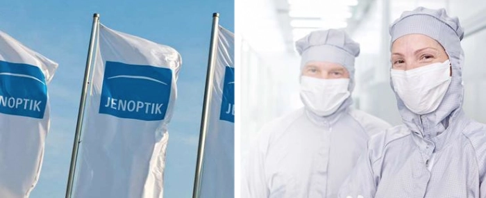
Jenoptik invests at Berlin Adlershof Technology Park
Jenoptik is equipping its Berlin location with further new high-tech facilities and is preparing itself for the planned capacity expansion of semiconductor material for high-power diode lasers.
The production site in Berlin Adlershof specialises in semiconductor laser manufacturing. The production line includes epitaxy, wafer processing and facet coating. Investments are currently being made primarily in the front-end process of wafer processing and in facet coating.
Jenoptik will commission new metallisation plants for wafer processing by the beginning of 2020 at the latest. These machines enable various metal layers to be applied to semiconductors by vapour deposition or sputtering. In addition, the so-called lift-off process will be modernised with a new machine. This serves to remove the photoresist mask after exposure on the semiconductors. For the final process step, the facet coating, Jenoptik will also be using a new plant and, simultaneously, a new technology starting in the fall of 2019. This will contribute more strongly to the stabilisation and higher output power of laser bars, a press release states.
“With the new investments, we want to expand the total production capacity, increase the value added in the process chain and accelerate the worldwide order processing of lasers”, says site manager Dr. Jürgen Sebastian.
Jenoptik’s semiconductor laser bars are mainly used in the fields of medical technology and life science, as well as for advanced manufacturing technologies. The investments also serve to address new markets, such as LiDAR sensors in the automotive industry. In the same way, global research and development projects in Europe, Asia and the USA can also be supported thanks to the new production equipment.
