

© SMS
Electronics Production |
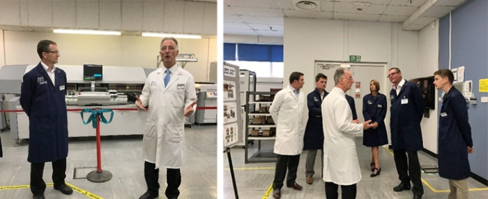
SMS opens UK based dedicated development centre for rapid NPI
The UK electronics company has officially opened the doors to ints new dedicated in-house Product Development Centre.
“SMS recognised that there was a gap in the market for product development services and the need to improve this crucial front-end service. Through our investment, we can demonstrate several improvements,” said Graham Shaw, SMS’ COO when detailing the reasons behind the company’s investment in a press release.
Firstly, SMS can now validate that the company can not only assemble the printed circuit boards but also provide its customers with the feedback on where performance improvements can be made.
“This collaborative process highlights, for our customer, how to effectively Design the product for Manufacturing, DFM, Manufacture for Cost, DFC, and Manufacture for Test, MFT, which enables the board to be developed faster, with no inherent quality issues or risks and, therefore, speeds up the entire process,” Mr. Shaw explains.
“Secondly, as we continuously listened to our customers and activated a critical assessment and audit with aerospace, defence, avionics and medical customers within the high-reliability sector, we had a need to have a secure and separate area. That is why we have created private and dedicated spaces for Analysis, Development, Test, and Stores that are all key coded for restricted and authorised only access,” Mr. Shaw continues.
Thirdly, over the past six years, SMS have made significant steps and investments to improve its capabilities in printing processes, vapor phase, and AOI. One might ask; why AOI in a prototyping environment?
Well, as Graham Shaw puts it: “even if you take away all the capacitors and resistors, we can automate the process simply, then all the development team need to focus on are the unique parts. Our investment in the Mycronic MY600 Jet Printer and the Mycronic MY200SX Placement is another example of our continued investment in making our operations smart.”
Lastly, SMS didn’t just want to have the capabilities to assemble PCB’s – the company also felt that there was a need for strong analytical capabilities.
“This is why, we invested our resources into creating a dedicated Analysis Laboratory to complement our Development Centre, whereby a product that is developed within our centre, will automatically flow through our process stream into the analysis lab. This is where we can go into the detailed examination, even as far as deconstructive testing to reduce our customer's overall risk and build their confidence in our overall manufacturing capabilities. This process also provides us with valuable data, educating, informing and advising us, keeping us within our continuous improvement roadmap,” Mr Shaw concludes.
