

© ic insights
Analysis |
Process roadmap for memory devices marches on as 3D looms
Vertical dimension to extend the life of DRAM and NAND flash as alternative memories get a closer look.
The ongoing reduction in feature sizes used to manufacture integrated circuits has enhanced memory-chip performance by increasing per-chip storage capacities, lowering power consumption, and improving the speed in which memory devices can store and retrieve data (i.e., memory bandwidth). For example, there has been a 20x improvement in the per-channel memory bandwidth of mobile DRAM over the past decade.
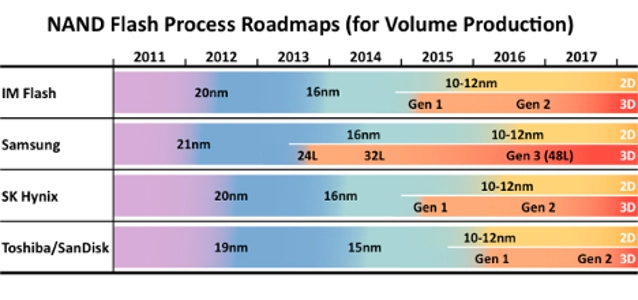
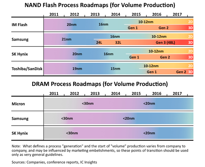
In mid-2014, the most advanced process technology used to make NAND flash devices was based on 20nm and smaller feature sizes, and just under 30nm for DRAMs. The process technology roadmaps shown in Figure 1 suggest that by 2017, the minimum feature size for 2D (planar) NAND flash will migrate to 10-12nm and to ≤20nm for DRAM. The transition points shown in the chart should be used only as rough guidelines since reported minimum feature sizes and mass production definitions are very imprecise and may be influenced by marketing “numbers games” as companies strive to get ahead of the competition.
In manufacturing NAND flash memory, companies such as Samsung, SK Hynix, Toshiba, and IM Flash Technologies are currently applying minimum geometries of 15-16nm. The first of these NAND devices were built in 2H13, but production quantities were limited amid reports of initial yield challenges. However, high-volume production of 15-16nm NAND chips has been ramping up in 2014.
SanDisk announced that the generation following its 19nm-based NAND chips (some call it the 1y generation that follows 1x) would have the same minimum geometry (19nm) as the prior generation. It was expected that SanDisk’s 1y NAND chips would have a minimum geometry of 15-16nm. Though the minimum feature size remained the same, SanDisk was able to reduce the memory cell size by 25%. Initial production of the 1y devices started in the second half of 2013. It appears that SanDisk (and its manufacturing partner Toshiba) decided to improve the cell size through advanced memory cell design efforts instead of scaling the geometry.
IM Flash, the memory-chip joint venture between Intel and Micron, said it believes two-dimensional NAND flash technology could be scaled to 10nm and that 3D NAND would take over from there. The company also said that 3D NAND would have to be manufactured with at least 32 layers to be economically feasible.
 © IC Insights
The first company to mass-produce 3D NAND chips was Samsung. In May 2014, the company announced that it had started volume production of its V-NAND flash chips using 32 memory cell layers. The company had previously shipped a limited number of solid-state drives (SSDs) based on its first generation 24-layer V-NAND technology to some of its data center customers in 2013. In conjunction with the 32-layer V NAND announcement, Samsung launched a line-up of premium SSDs based on the second-generation technology that are available for not just data center applications, but also for high-end personal computers.
Other NAND flash manufacturers are hoping to begin production of 3D NAND parts in 2014, but 2015 appears more likely. Manufacturing 3D NAND is incredibly complex and there still are issues being worked out, so as long as life remains in traditional planar-transistor NAND devices, 3D NAND technology will not be rushed into the marketplace. The timing of a full-scale transition from 2D to 3D NAND memory depends a great deal on the point at which 3D becomes a cost-effective option to 2D, and that situation is still a ways off. Even when the cost crossover point is reached, 2D and 3D NAND will likely coexist for several years.
For about the past 10 years, DRAM devices have been a generation or more behind NAND flash memories when it comes to process technology, if the minimum geometry of each process is used for comparison. Leading DRAM makers are currently manufacturing at volume production using 20nm-class feature sizes (between 20-29nm).
DRAM and NAND processes are less similar than one might think, and each has its own figures of merit and scaling limitations. Nevertheless, NAND has generally been considered the more advanced of the two memory technologies ever since Samsung announced in 2003 that NAND had taken over for DRAM as the driver of the company’s memory-related process advancements.
Like NAND flash, DRAM technology is also migrating toward integrating circuitry in the vertical direction, but the 3D technology pertaining to DRAMs is different than that of NAND flash. In general, 3D technology for DRAMs involves the creation of stacks of DRAM chips interconnected using thru-silicon vias (TSVs). One example of a 3D DRAM solution is the Hybrid Memory Cube (HMC), developed by the consortium of the same name. The Hybrid Memory Cube Consortium was founded by Micron and Samsung and includes other developer members Altera, ARM, IBM, Open-Silicon, SK Hynix, and Xilinx.
DRAM consumption for mobile and server applications has been on the rise in recent years, prompting suppliers to develop creative techniques to extend the life of this memory technology. Between 2010 and 2014, three generations of Intel server processors have been introduced with the 22nm Haswell (the most current offering) featuring up to 15 cores and integrated high-speed memory controllers that can support up to 6TB (terabytes) of DRAM.
Intel’s Haswell has the capability to address three times as much memory compared to its 32nm Westmere processor in 2012 and five times as much memory compared to its 45nm Nehalem processor in 2010, which is one of the big reasons why DRAM suppliers are busy working to boost chip density and performance (speed) of their new DRAM devices.
© IC Insights
The first company to mass-produce 3D NAND chips was Samsung. In May 2014, the company announced that it had started volume production of its V-NAND flash chips using 32 memory cell layers. The company had previously shipped a limited number of solid-state drives (SSDs) based on its first generation 24-layer V-NAND technology to some of its data center customers in 2013. In conjunction with the 32-layer V NAND announcement, Samsung launched a line-up of premium SSDs based on the second-generation technology that are available for not just data center applications, but also for high-end personal computers.
Other NAND flash manufacturers are hoping to begin production of 3D NAND parts in 2014, but 2015 appears more likely. Manufacturing 3D NAND is incredibly complex and there still are issues being worked out, so as long as life remains in traditional planar-transistor NAND devices, 3D NAND technology will not be rushed into the marketplace. The timing of a full-scale transition from 2D to 3D NAND memory depends a great deal on the point at which 3D becomes a cost-effective option to 2D, and that situation is still a ways off. Even when the cost crossover point is reached, 2D and 3D NAND will likely coexist for several years.
For about the past 10 years, DRAM devices have been a generation or more behind NAND flash memories when it comes to process technology, if the minimum geometry of each process is used for comparison. Leading DRAM makers are currently manufacturing at volume production using 20nm-class feature sizes (between 20-29nm).
DRAM and NAND processes are less similar than one might think, and each has its own figures of merit and scaling limitations. Nevertheless, NAND has generally been considered the more advanced of the two memory technologies ever since Samsung announced in 2003 that NAND had taken over for DRAM as the driver of the company’s memory-related process advancements.
Like NAND flash, DRAM technology is also migrating toward integrating circuitry in the vertical direction, but the 3D technology pertaining to DRAMs is different than that of NAND flash. In general, 3D technology for DRAMs involves the creation of stacks of DRAM chips interconnected using thru-silicon vias (TSVs). One example of a 3D DRAM solution is the Hybrid Memory Cube (HMC), developed by the consortium of the same name. The Hybrid Memory Cube Consortium was founded by Micron and Samsung and includes other developer members Altera, ARM, IBM, Open-Silicon, SK Hynix, and Xilinx.
DRAM consumption for mobile and server applications has been on the rise in recent years, prompting suppliers to develop creative techniques to extend the life of this memory technology. Between 2010 and 2014, three generations of Intel server processors have been introduced with the 22nm Haswell (the most current offering) featuring up to 15 cores and integrated high-speed memory controllers that can support up to 6TB (terabytes) of DRAM.
Intel’s Haswell has the capability to address three times as much memory compared to its 32nm Westmere processor in 2012 and five times as much memory compared to its 45nm Nehalem processor in 2010, which is one of the big reasons why DRAM suppliers are busy working to boost chip density and performance (speed) of their new DRAM devices.