


© Linear Technology
General |
Power Supply Layout and EMI
PC-board layout determines the success or failure of every power supply project. It sets functional, electromagnetic interference (EMI), and thermal behavior.
EDITOR'S NOTE_ All graphics © Linear Technology / All graphics have a Zoom-funktionIntroduction PC-board layout determines the success or failure of every power supply project. It sets functional, electromagnetic CIN interference (EMI), and thermal behavior. Switching power supply layout is not black magic, but is often overlooked until it is too late in the design process. Fortunately physics is on your side. Functional and EMI requirements must be met, and in a world of trade-offs in power supply unit layout, what is good for functional stability is good for EMI. Good layout from first prototyping on does not add to cost, but actually saves significant resources in EMI filters, mechanical shielding, EMI test time and PC board runs. This application note focuses primarily on nonisolated topologies, but will examine some isolated topologies as well. You will learn to make the optimum choices regarding PC-board layout for solid power supply designs. I remember about a dozen years ago as a customer was using a switch mode power supply in a car radio for the first time many of his colleagues said that it could not be done. However, after a few things were ironed out in layout and input filtering, everything worked fine. Later a customer successfully used an LT1940 1MHz dual step- down switching regulator, which operated in the middle of his AM band in a car radio receiver. No additional metal shielding was required for the power supply unit (PSU); it was only an issue of placement and layout. In order to get there, we need to go through some physics.
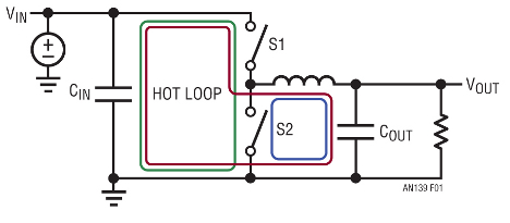
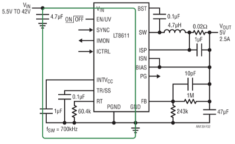
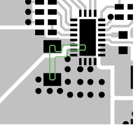
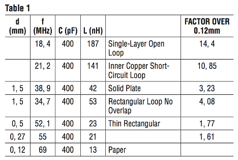
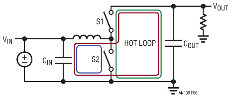
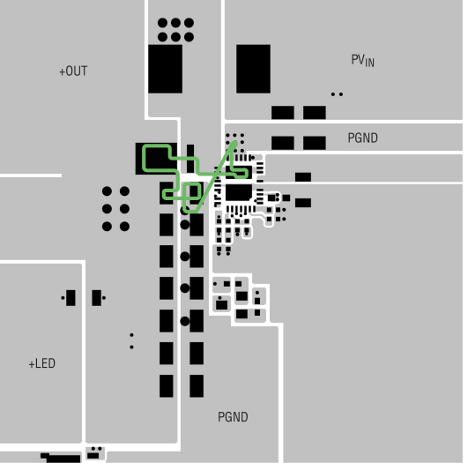
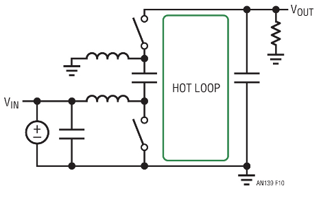
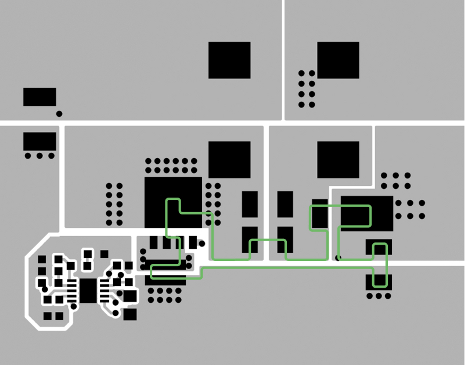
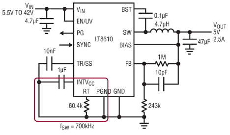
With nonisolated topologies, one of the most basic topolo- gies is the buck regulator. EMI starts off from high di/dt loops. The supply wire as well as the load wire should not have high AC current content. So we can focus our analy- sis from the input capacitor, CIN, which should source all relevant AC currents to the output capacitor, COUT, where any AC currents end. During the ON cycle with S1 closed and S2 open, the AC current follows the red loop (Figure 1). During the off cycle, with S1 open and S2 closed, the AC current follows the blue loop. Both currents have a trapeze shape. People often have difficulty grasping that the loop producing the highest EMI is not the red nor the blue loop. Only in the green loop flows a fully switched AC current, switched from zero to IPEAK and back to zero. We refer to the green loop as a hot loop, since it has the highest AC and EMI energy. In order to reduce EMI and improve functionality, you need to reduce the radiating effect of the green loop as much as possible. If we could reduce the PC-board area of the green loop to zero and buy an ideal input capacitor with zero impedance, the problem would be solved. But we are limited to the real world. The task of engineering is to find the optimal compromise. Let’s take a look at the layout of an LT8611 buck converter (Figure 3). The LT8611 has both switches internal, so we only have to be concerned with the connection of the input capacitor. As you can see from the schematic in Figure 2, the hot loop is not easy to spot for layout purposes. The green line is the hot loop in the top layer. AC current flows through the input capacitor and the switches in the part. Figure 3 shows the DC1750A LT8611 demo board. The current density in the cross cut of the hot loop will look like this (Figure 4). How much does a copper short-circuit loop or plane under the hot loop improve the functional and EMI behavior of your circuit? The result of an experiment with a 10cm × 10cm rectangular loop with 27MHz is shown in Table 1. The table gives an indication how much improvement a solid copper plane under the hot loop topside traces gives. The first line is no plane single layer. The inductance of a single-layer loop of 187nH gets down to 13nH in the case of only 0.13mm insulation between the plane and loop traces. A solid plane on the next layer in a multilayer board (four layers or more) will have over 3× less inductance than a normal 1.5mm 2-layer board with a solid bottom plane, and over 14× less over a single-layer board. A solid plane with minimum distance to the hot loop is one of the most effective ways to reduce EMI.Figure 1 -----
Figure 2 -----
Figure 3 -----
Figure 4 -----
Figure 5
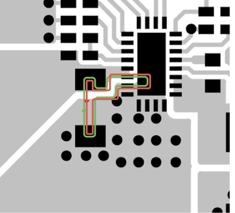
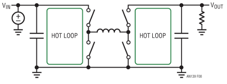
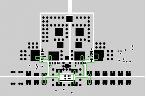
Where Does the Current Flow in the Plane? The green top layer hot loop magnetic AC field produces eddy currents in the plane (Figure 5). Those eddy currents produce a mirror AC magnetic field, which is opposite the hot loop field (red trace). Both magnetic fields will cancel out. This works better the closer the mirror current is to the hot loop. Current is a round trip in the top layer. The most likely current path in the shield is the same round trip direct under the top layer. Both currents are almost the same. Since the plane current needs to be as high as the top trace current, it will produce as much voltage across the plane as is necessary to sustain the current. To the outside it will show up as GND bounce. From EMI perspective small hot loops are best. A power supply IC with integrated sync switches, optimized pinout and careful internal switch control will outperform on EMI a non-sync power supply IC with external Schottky diode. And both will outperform a controller solution with external MOSFETs. The boost circuit can be viewed in continuous mode as a buck circuit operating backwards. The hot loop is identified as the difference between the blue loop if S1 is closed and the red loop (Figure 6) with S1 open and S2 closed. The hot loop of the LT3956 LED driver boost controller is shown in green (Figure 7). The second layer is a solid GND plane. The main EMI emitter is the magnetic an- tenna the hot loop creates. The area of the hot loop and its inductance are tightly related. If you are comfortable thinking in inductance, try to decrease it as much as you can. If you are more comfortable in antenna design, reduce the effective area of the magnetic antenna. For near field purposes, inductance and magnetic antenna effectiveness are essentially the same. The single inductor 4-switch buck-boost (Figure 8) consists of a buck circuit followed by a boost circuit. The layout will often be complicated by a common GND current shunt which belongs to both hot loops. The LTC3780 DC1046A demo board (Figure 9) shows an elegant solution splitting the sense resistor in two parallel ones. A bit different drawing of a SEPIC circuit (Figure 10) shows its hot loop. Instead of an active MOSFET for the top switch, a diode is often used. The LT3757 DC1341A (Figure 11) shows a good SEPIC layout. The green hot loop area is minimized and has a solid GND plane on the next layer. The inverting topology (Figure 12) is very similar to SEPIC, only the load has moved through the top switch and top inductor. Layout is very similar, and demo boards can typically be modified from SEPIC to inverting provided the IC can also regulate on negative feedback voltage like LT3581, LT3757 etc..Table 1 -----
Figure 6 -----
Figure 7 -----
Figure 8 -----
Figure 9
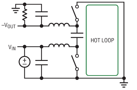
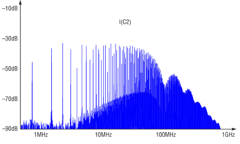
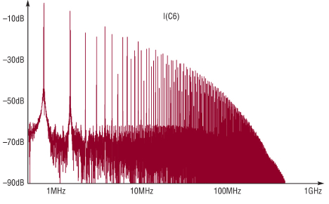
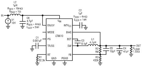
Flyback (Figure 13) uses separate windings on a trans- former and there is only magnetic coupling between the primary and secondary windings. The current in the primary winding goes to zero at a relative high di/dt; only the energy stored in the leakage inductance and capacitance between windings and on the switch node slows that down. The primary and other transformer windings can be seen as fully switched current. We get two main hot loops as in the buck-boost case (Figure 8). To reduce EMI, in addition to close VIN decoupling for differential mode EMI, common mode chokes are used for the likely dominant common mode EMI in this topology. Other AC Loops The hot loop with the main switching energy is the major source of RF energy. However for the operation of the IC and circuit, other AC carrying loops are required. All circuits need a supply for the main switch driver. In the case of the buck, it is often decoupled with the same VIN capacitor as the hot loop. Other ICs use a separate voltage for the drive circuit, often referred to as INTVCC (Figure 14). Make the INTVCC capacitor PGND and GND loop as small as possible and shield it with a solid plane in the next layer. EMI energy is on the order of 20dB lower than in the main hot loop. Any excessive inductance in the INTVCC loop will deteriorate IC performance. The INTVCC capacitor decouples beside switch drive internal sensitive and wide band circuitry like current sense comparators, reference and error amplifiers which are very often internal supplied from INTVCC too. Figure 15 is an FFT of the current in the INTVCC decoupling capacitor (C2 in Figure 17). Figure 16 is an FFT of the current in the input capacitor (C6 in Figure 17). The RF energy is over 20dB higher than in the INTVCC loop. The LT8610 LTspice circuit (Figure 17) L2 with a high loss of RPAR = 1Ω is used to decouple the zero impedance LTspice voltage source, V1, from the input capacitor, C6. Note: LTspice switch mode regulator models are developed to simulate the functionality of the IC. Use great caution to extrapolate RF behavior because the models do not account for the internal or the external lump devices or board layout. However, it is nonetheless a great tool to get an approximation of very difficult to measure effects. External Switch Drive Signals After the main hot loop and the INTVCC decoupling loop, the next EMI trouble sources are often external switch drive signals. Even modern MOSFETs have single-to-dual digit nanofarad effective input capacitance.Figure 10 -----
Figure 11 -----
Figure 12 -----
Figure 13 -----
Figure 14
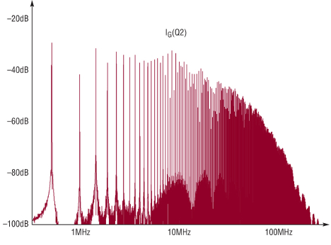
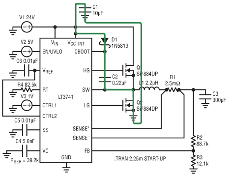
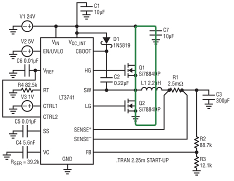
Their drivers often have drive currents in the single amp range, with rise and fall times approaching single digit nanoseconds. Figure 18 is the FFT of the gate current into Q2 of Figure 19. The green loop (Figure 19) shows the current path for the bottom gate current. It is supplied from the C1. Make sure that the loop is small. The Q2-source GND to C1 GND connection is most easily accomplished with a solid GND area in the next layer under the component layer. The red and green loop (Figure 20) shows the top gate drive current loops. They are supplied from the boost capacitor, C2, and the return is the SW connection to the controller IC. Keep the red loop small and place the traces parallel with only a small gap. If C2 is placed close to the controller IC, the green loop will also become small. The green loop (Figure 21) shows the recharge of the boost capacitor. If you have already made the above loops small and have placed D1 relatively close, this loop is also small. Passive antennas, including magnetic antennas or loops, operate reciprocally, and their transmit and receive char- acteristics are the same. The sense amplifier in Figure 22 looks with high bandwidth at SENSE+ and SENSE– on the small shunt voltage over R1 to terminate the top switch on cycle. Even sub-millivolt noise will result in duty cycle jitter. Coupling to any of the former transmitting loops should be minimal. First, this loop area needs to be small as well, so make the gap between the SENSE+ and SENSE– line minimal. Then place the loop traces on the other side of a shielding plane from the high current loops mentioned above. If enough layers are available, the SENSE+ and SENSE– line can be on top of each other if there are not significant magnetic AC fields parallel to the PC board layers. If SENSE+ and SENSE– filtering is used, place the filter close to the controller IC, since R1 is always low impedance and the sense inputs are higher impedance. The main hot loop in Figure 23 consists of the external MOSFETs Q1 and Q2 and the closest low impedance de- coupling capacitor C7. This is the loop with the highest RF energy in a controller solution. How Shielding Works DC magnetic fields go through air, FR4 epoxy dielectric and copper almost undisturbed. AC magnetic fields are impacted only by the induced cur- rents in a conductor—usually copper or tin, etc. So, absent from ferromagnetic material, we can focus on currents as the only source to alter or attenuate AC magnetic fields in a typical PC board environment. We know from experiments that complete conductive enclosures have a very high attenuation—easily over 100dB—over a very broad frequency range above the AM band. Cookie boxes are a popular example widely used in the R&D community to shield sensitive circuitry, to en- able high frequency (HF) measurements.Figure 15 -----
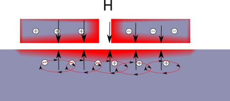
Figure 16 -----
Figure 17 -----
Figure 18 -----
Figure 19

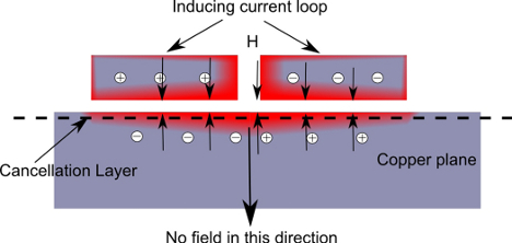
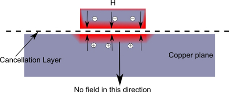
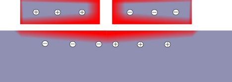
For HF circuits you can buy them in rectangular form which fits easier for PC boards and HF connectors like BNC, N, SMA, etc. For practical purposes HF magnetic fields do not escape closed conductive boxes as long as the wall is thicker than skin depth. If we blow up the conductive enclosure like a balloon large enough that it is a flat wall between us and the AC current, the eddy currents in the shield material need to create an AC magnetic field, which is the opposite of the original AC current behind the wall (Figure 24). The eddy currents in the shield will only be enough to cancel any magnetic AC field to the outside of the box or, in our case, in the direction shown at the lower portion of Figure 25. How Effective is a Shield? If the board copper plane were non-conductive, it would be transparent to any magnetic field like a sheet of paper. The current in the copper is the only source of influence on the magnetic field. The energy available for eddy cur- rents is induced in the shield. Such currents will cancel any magnetic field inside the copper shield and outside in the direction away from the inducing current, within the limits of skin and proximity effect (Figure 26). The cancellation layer is the layer that cancels the mag- netic field from the inducing currents (i.e., from the hot loop) and induced currents in the shield. So it is sort of midway between the AC currents in opposite directions. The position of the cancellation layer can be estimated by rule of thumb and may help you visualize how the remaining AC fields look. The closer the cancellation layer is to the induced current layer, the better the cancellation. Inductance is the integral of the magnetic field—the same magnetic field that forms the near field RF antenna. All of these effects are reduced when the cancellation layer is placed closer to the inducing current loop. What Works Even Better? If the current returns through the plane, the situation is somewhat different (Figure 27). Now the current in the plane is not only passive induced, but is the active return flow. It is forced to be same as the current in the top trace. The benefit is that the cancellation is now closer to the inducing trace, in this case halfway between the top layer current and the returning current in the plane. Because the cancellation layer is now half the distance to the inducing current, it is safe to say that the magnetic field is now lower by at least a factor of two compared to the above situation with passive shielding only. If you can, let the return current flow in the closest layer. Make its dielectric (isolation) as thin as practical. It is better to have the return current flow in the closest trace to the inducting current with minimum dielectric distance. That’s what solid GND planes do by default. Standard multilayer boards often have much thinner outer layer dielectrics to help reduce EMI.Figure 20 -----
Figure 21 -----
Figure 22 -----
Figure 23 -----
Figure 24


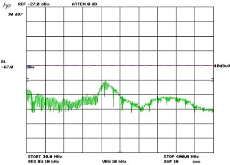
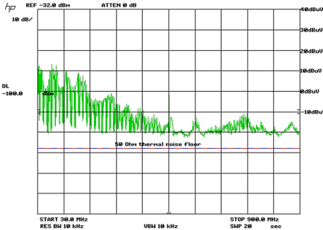
Line Conducted EMI Measurements Figure 28 is an LT8611 with some input filtering with a fer- rite bead and 4.7μF ceramics line conducted from 30MHz to 400MHz. The display line of –67dBm corresponds to 40dBuV. Figure 29 shows an LT8610 power supply 13V in, 5V out at 1A out, line conducted up to 900MHz. In Figure 29 an additional wideband amplifier (LNA) in the HF signal chain with 35dB gain is used. So the –100dBm spectrum analyzer display line corresponds to –135dBm, which is the thermal noise floor of a 50Ω system with 10kHz bandwidth at room temperature. The main HF energy needed to be filtered out of the LT8610/LT8611 is below 400MHz. +10dBuV corresponds to 3.16μVRMS. EMI Optimization First check the layer stack. Use a PC board of four layers or more if possible. The second layer from top is typically only about 200μm distance, and a shield will cancel the hot loop much better than any shield over 1mm away in a dual layer board. In the hot loop shield, the same current as in the top trace hot loop runs as eddy current. Keep the layer 2 shield solid. Place vias away from the hot loop for connections to GND planes you want to keep quiet. The hot loop shield cancellation currents create HF voltage across the loop, and you do not want to couple it with vias in areas you need quiet. This current decays with distance, but often remains a problem. The challenge for filtering the input and, if required, the output is mainly in finding an area that is quiet enough. An effective way is to make a complete GND ring around the the power supply unit (PSU) connected with vias. Filter capacitor GND return should be at the location where the VIN current crosses the ring. There should be still filtering inductance in the direction of the hot loop. That can be a ferrite bead or an inductor. Beware of magnetic coupling between filter inductors and the main inductor. The transformer action can jeopardize your attenuation. Place filter inductors at a distance from the main inductor. Use short ceramic capacitors, i.e., 0402, or reverse ge- ometry capacitors because the block capacitors need low equivalent series inductance (ESL) which mainly dictates their impedance. Shorter and thicker ones have lower ESL. Characteristic impedance of the strip lines you create with your VIN traces is in the low single digit Ohm area. The ESL of your block capacitors should be as low as possible. Use reverse geometry capacitors or a stack of 0402 closest to the filter point and larger cases close by. Any trace length significantly increases the few hundred pH inductance your small block capacitors have. Ensure that the routing path of the VIN and the return trace go through the filter capacitor pads. This avoids additional trace inductance. ----- Author: Christian Kück, Linear Technology CorporationFigure 25 -----
Figure 26 -----
Figure 27 -----
Figure 28 -----
Figure 29