
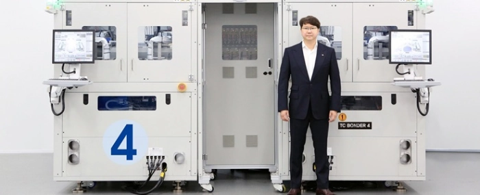
HANMI Semiconductor launches TC BONDER 4 for HBM4
TC BONDER 4 is dedicated equipment capable of HBM4 production, featuring significantly improved productivity and precision compared to competitors, tailored to the characteristics of HBM4 which requires even higher precision.
South Korean chip packaging equipment maker HANMI Semiconductor has announced the launch of TC BONDER 4, dedicated equipment for next-generation AI semiconductor HBM4 production.
Some industry experts had suggested that Hybrid Bonding technology would be necessary for HBM4 production. However, when the Joint Electron Device Engineering Council (JEDEC) relaxed the HBM4 standard height to 775 micrometers, HANMI expected to directly benefit as manufacturing HBM4 with TC BONDER equipment became possible, according to a media release.
“The global HBM market is growing explosively every year due to the rapid growth of the AI market,” said Kwak Dong Shin, Chairman of HANMI Semiconductor. “HANMI Semiconductor’s world-leading market share and competitiveness in HBM TC BONDERs remain unchanged.”
He added that NVIDIA’s next-generation product, Blackwell Ultra, which will be introduced in the second half of this year, will also be produced using HANMI Semiconductor’s TC BONDER.
TC BONDER 4 is dedicated equipment capable of HBM4 production, featuring significantly improved productivity and precision compared to competitors, tailored to the characteristics of HBM4 which requires even higher precision, Kwak said.
“It will be actively utilized in global semiconductor customers’ HBM4 production and will significantly contribute to sales as the HBM4 market expands in the future,” Kwak added.
Memory companies worldwide are preparing for mass production of HBM4 in the second half of this year. HBM4, the sixth-generation high-bandwidth memory, boasts innovative performance with 60% improved speed compared to the fifth-generation (HBM3E) while reducing power consumption to 70% of previous levels. It supports up to 16 layers and expands DRAM capacity per chip from 24Gb to 32Gb. The number of Through-Silicon Via (TSV) interfaces, which serve as data transfer pathways, has also increased to 2048, double that of the previous generation, enhancing data transfer speeds between processors and memory, the media release said.
As the importance of high-difficulty bonding technology increases in HBM stacking processes requiring high precision for 16 or more layers, HANMI Semiconductor’s TC BONDER is expected to play a key role in determining the quality of HBM stacking, the South Korean company said.