

© Tensilica
Electronics Production |
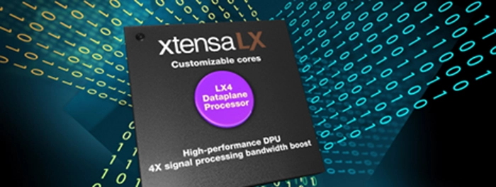
Tensilica IP Core for dataplane & signal processing functions
Tensilica stages new Xtensa LX4 dataplane processor (DPU) for SOCs (system-on-chips).
The new Xtensa LX4 DPU supports wider local data memory bandwidth of up to 1024 bits per cycle, wider VLIW (very long instruction word) instructions up to 128 bits for increased parallel processing, and a cache memory prefetch option that boosts overall performance for systems with long off-chip memory latency. Tensilica is already using many of these capabilities in its recently introduced ConnX BBE64 DSP for LTE Advanced communications.
"The strength of Tensilica's DPUs is the ability to combine control and digital signal processing functions in cores that can be optimized to provide 10x to 100x performance improvement compared to a standard RISC or DSP core," stated Steve Roddy, Tensilica's vice president of marketing and business development. "Now, with Xtensa LX4, Tensilica offers IP cores that range from an ultra-small programmable DPU as exemplified by a 1GigaMAC-per-second DSP in 0.01mm2 (in 28 nm process technology) up to the ConnX BBE 64-128, the world's highest performance licensable DSP IP core with over 100 GigaMAC per second performance."
Availability and Performance
The Xtensa LX4 DPU is available now from Tensilica. The base Xtensa LX4 DPU can reach speeds of over 1 GHz in 45 nm process technology (45GS) with an area of just 0.044 mm2.