


Sponsored content by CML

How Prepared Are You for Geometric Dimensioning & Tolerance?
One of the biggest challenges that PCB manufacturers face, though it may seem simple but is often overlooked: missing essential information that describes the product. The purpose of PCB drawings is to visualize the representation of a product completely and precisely for production. The PCB drawings today appear more like mechanical drawings for engines rather than for electronic components. Changing a drawing is not a big problem, but to change it when it is already released in production, can create considerable extra expenditures due to delay in production and wrong material selection. However, these problems can be easily avoided.
When the DIN EN ISO 8015 was released in 2011, it was not a big topic in the PCB industry.
The PCB drawings were simple and clearly arranged. The tolerances, such as ±0.1mm, could be understood by everyone around the world and the result of measurement told us exactly where the deviation from the reference value was.
Another fact is the development software for PCB. Today more and more companies use 3D CAD tools to create the complete PCB specification and documentation.
The PCB drawings today appear more like mechanical drawings for engines rather than for electronic components. Topics like Geometric Dimensioning & Tolerance (GD&T) also known as Geometrical Product Specification (GPS) and ISO 8015 are coming up and various symbols and their meanings are often not clear.
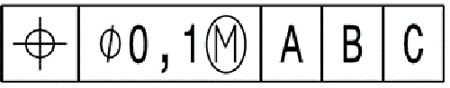 Image 01: position accuracy requirement with round tolerance zone and MMC (maximum material condition)
GD&T is a common set of rules and definitions used on engineering drawings and models to define the allowable deviation of feature geometry. It enables engineers and designers to communicate what they require with regards to the product design. Then manufacturers use GD&T to understand the design to determine the set-up requirements for production. GD&T involves dimensions, tolerances, symbols, definitions, rules, and conventions that can be used to precisely convey the requirements for the location, orientation, size, and form of each feature of the product.
Image 01: position accuracy requirement with round tolerance zone and MMC (maximum material condition)
GD&T is a common set of rules and definitions used on engineering drawings and models to define the allowable deviation of feature geometry. It enables engineers and designers to communicate what they require with regards to the product design. Then manufacturers use GD&T to understand the design to determine the set-up requirements for production. GD&T involves dimensions, tolerances, symbols, definitions, rules, and conventions that can be used to precisely convey the requirements for the location, orientation, size, and form of each feature of the product.
 The drawing’s purpose is to completely and precisely visualize the representation of a product so that the manufacturer knows all the requirements to produce the product. According to official studies [Jor 17] around 80% of all drawings are either incomplete or ambiguous.
One of the biggest challenges that PCB manufacturers face, though it may seem simple but is often overlooked: missing essential information describing the product. Changing a drawing at this stage of the product life cycle is not a big problem. But it is costly to change the drawing when it is already released for production. To change the drawings that are already released in production can create considerable extra expenditures due to delay in production and wrong material selection. However, these problems can be easily avoided.
At CML, we are more than well prepared for the coming challenges of today’s production drawings and ready to help you fulfil your mission.
Find out more on how to prepare for GD&T here.
Reference:
[Jor 17] Jorden, W. und Schuette W.: Form- und Lagetoleranzen - Handbuch fuer Studium und Praxis; 9. Aufl. 2017, S.14
The drawing’s purpose is to completely and precisely visualize the representation of a product so that the manufacturer knows all the requirements to produce the product. According to official studies [Jor 17] around 80% of all drawings are either incomplete or ambiguous.
One of the biggest challenges that PCB manufacturers face, though it may seem simple but is often overlooked: missing essential information describing the product. Changing a drawing at this stage of the product life cycle is not a big problem. But it is costly to change the drawing when it is already released for production. To change the drawings that are already released in production can create considerable extra expenditures due to delay in production and wrong material selection. However, these problems can be easily avoided.
At CML, we are more than well prepared for the coming challenges of today’s production drawings and ready to help you fulfil your mission.
Find out more on how to prepare for GD&T here.
Reference:
[Jor 17] Jorden, W. und Schuette W.: Form- und Lagetoleranzen - Handbuch fuer Studium und Praxis; 9. Aufl. 2017, S.14
Image 01: position accuracy requirement with round tolerance zone and MMC (maximum material condition)
GD&T is a common set of rules and definitions used on engineering drawings and models to define the allowable deviation of feature geometry. It enables engineers and designers to communicate what they require with regards to the product design. Then manufacturers use GD&T to understand the design to determine the set-up requirements for production. GD&T involves dimensions, tolerances, symbols, definitions, rules, and conventions that can be used to precisely convey the requirements for the location, orientation, size, and form of each feature of the product.
The drawing’s purpose is to completely and precisely visualize the representation of a product so that the manufacturer knows all the requirements to produce the product. According to official studies [Jor 17] around 80% of all drawings are either incomplete or ambiguous.
One of the biggest challenges that PCB manufacturers face, though it may seem simple but is often overlooked: missing essential information describing the product. Changing a drawing at this stage of the product life cycle is not a big problem. But it is costly to change the drawing when it is already released for production. To change the drawings that are already released in production can create considerable extra expenditures due to delay in production and wrong material selection. However, these problems can be easily avoided.
At CML, we are more than well prepared for the coming challenges of today’s production drawings and ready to help you fulfil your mission.
Find out more on how to prepare for GD&T here.
Reference:
[Jor 17] Jorden, W. und Schuette W.: Form- und Lagetoleranzen - Handbuch fuer Studium und Praxis; 9. Aufl. 2017, S.14