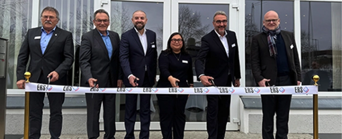
ERS electronic opens production and R&D facility in Germany
ERS electronic, a specialist in thermal management solutions for semiconductor manufacturing, has officially opened ERS Barbing, its new production and R&D facility, coupled with a cutting-edge Competence Center for Advanced Packaging and Advanced Backend technologies.
Located in Barbing near Regensburg, this new facility is designed to accelerate process development and production of ERS's renowned Advanced Packaging equipment.
Additionally, the integrated Competence Center offers customers direct access to ERS's technical expertise in wafer and panel debonding, as well as warpage handling and measurement, enabling hands-on testing, demonstrations, and collaborative innovation.
"The opening of this facility underscores our dedication to advancing semiconductor technologies and supporting our customers in Europe and beyond," says Laurent Giai-Miniet, CEO of ERS electronic, in a press release. "Through firsthand demonstrations and personalized support, we aim to help our customers accelerate time-to-market and optimize manufacturing processes."
By investing in this facility, ERS reinforces its role as a key contributor to the European semiconductor industry, aligning with regional initiatives to strengthen competitiveness and boost supply chain resilience.
Imre Kosa, Site Manager of ERS Barbing, adds, "By combining production, R&D, and a Competence Center under one roof, we are empowering our partners with the tools and knowledge needed to drive innovation and meet the growing demands of the industry. We invite our partners and customers to visit and discover how our capabilities can help them overcome process challenges in debonding and warpage management."